 Products Home
自由空間用バイアスディテクター
- Monitor CW or Fast Pulsed Lasers
- Detectors for Wavelengths from 200 to 2600 nm
- Integrate with Cage or Lens Tube Systems
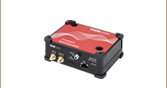
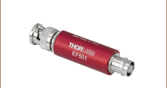
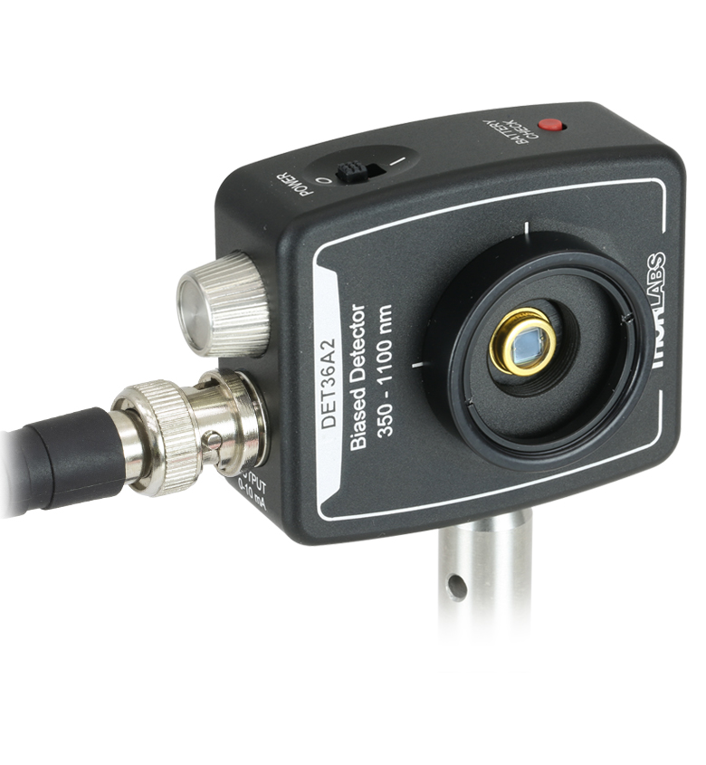
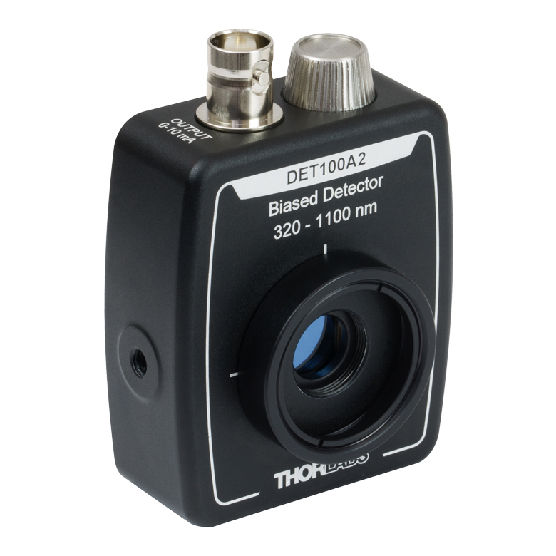
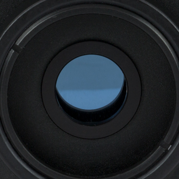
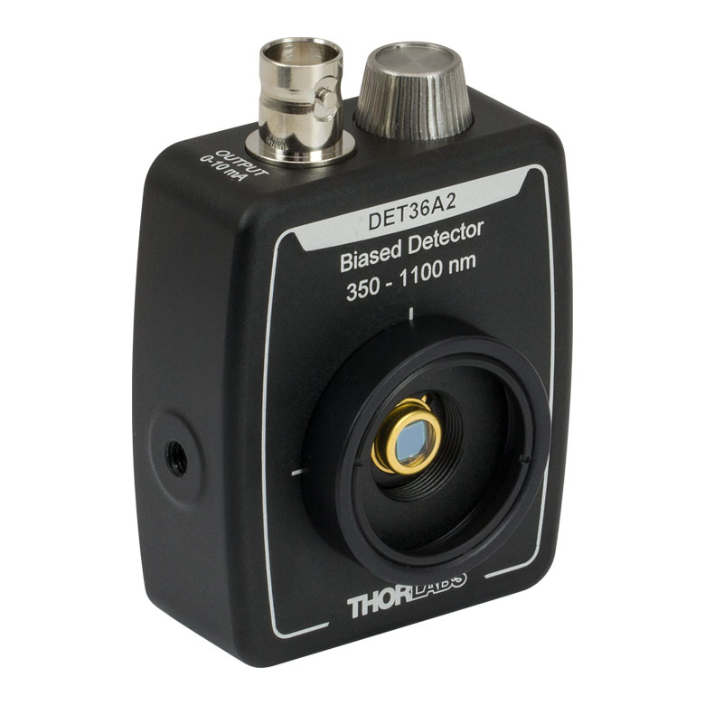
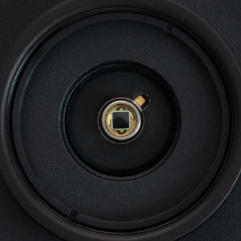
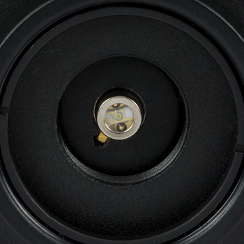
DET36A2
Biased Si Detector
Application Idea
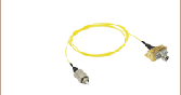
DET Series Detector Attached to a 30 mm Cage System Using the Included SM1 Coupler and an SM1T2 Adapter
(See the Housing Tab for Details)
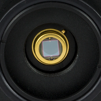
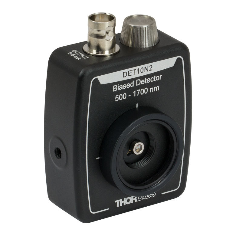
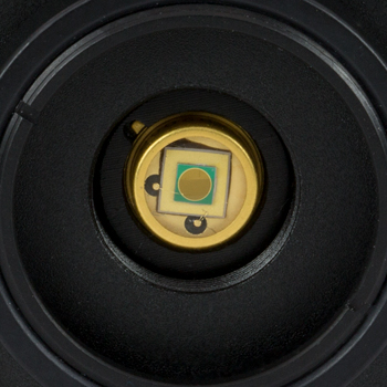
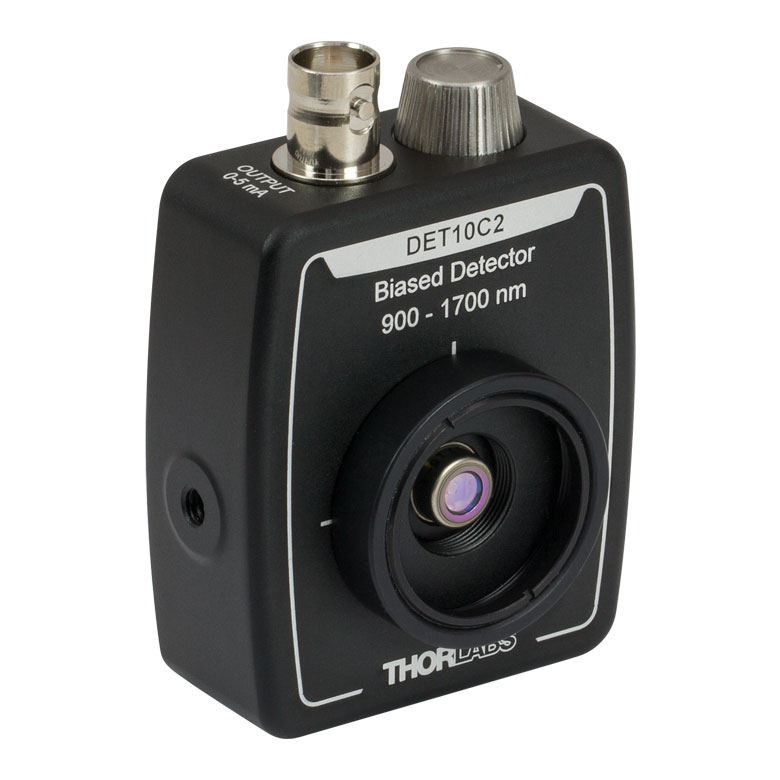
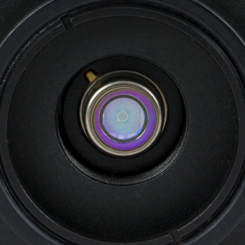
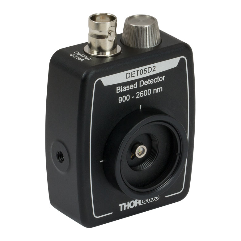
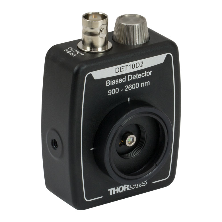
DET10D2
Biased InGaAs Detector


Please Wait
動作回路図
Click to Enlarge
ディテクタは、適用される入射光に対して線形の応答を生成するために逆バイアス状態になっています。
特長
- 200 nm~2.6 μmまでの波長をカバーするモデルをご用意
- 1 nsの高速立ち上がり時間
- 薄型で狭いスペースでの測定が可能
- SM05レンズチューブ、SM1レンズチューブ、ケージシステム、Ø12 mmまたはØ12.7 mmポストに取付け可能
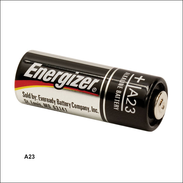
- 12 VDCのバイアス電池 A23内蔵
- その他の電源アダプタや電源もご用意(下記参照)
- SM1内ネジやSM1外ネジを使用してファイバ結合が可能
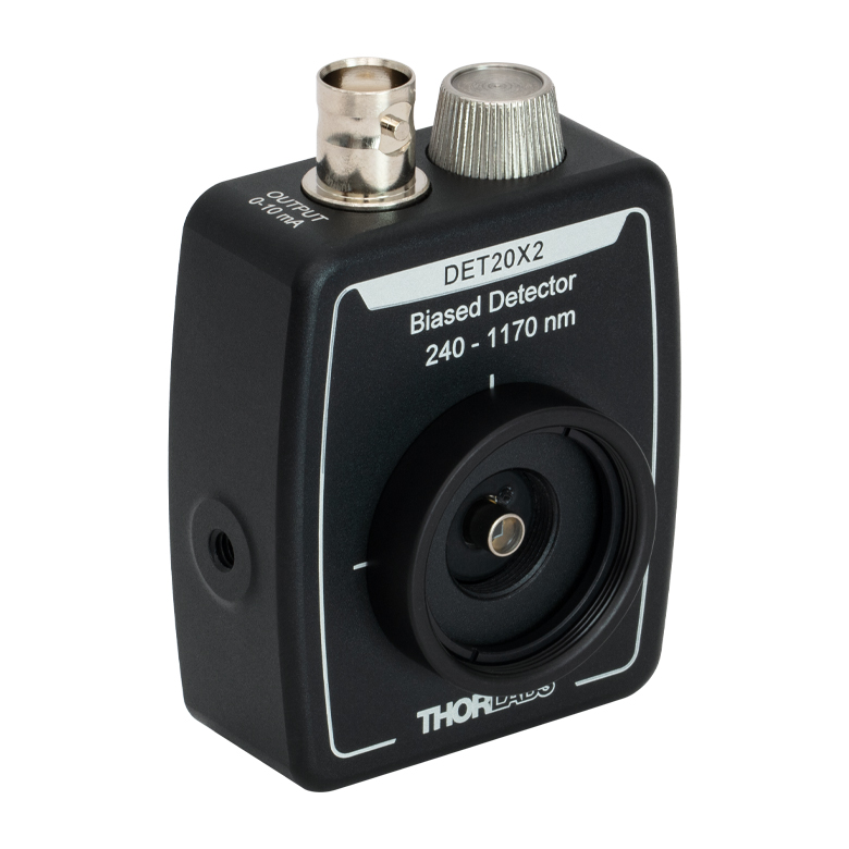
当社のバイアス型フォトディテクタは、UV域から中赤外域(200 nm ~2.6 µm)の波長範囲をカバーするモデルからお選びいただけます。 薄型筺体なので、光ディテクタを狭い領域にも挿入して使うことができます。当社のGeディテクタはN-on-P型のフォトダイオードをベースにしていますが、SiおよびInGaAsディテクタは高速PINフォトダイオードをベースにしています。各モデルは、丈夫なアルミニウム製筺体に高速PINフォトダイオードとバイアス電池が内蔵されています。当社のバイアスディテクタはベンチトップ型フォトダイオード増幅器およびPMTトランスインピーダンスアンプとお使いいただけます。
これらのディテクタは広帯域のDC結合出力により、高速パルスレーザやDC光源のモニタリングに適しています。 側面パネルにあるBNCには、フォトダイオードのアノード電流が直接出力されます。この出力は、終端抵抗を使って正の電圧へと簡単に変換できます。高速の信号を調べる際には、50 Ωの負荷抵抗器をご使用いただくことをお勧めしています。低帯域幅の用途では、可変ターミネータまたはスタブ型ターミネータをお使いいただくと測定電圧への迅速な調整が可能です。下記のディテクタは増幅器や利得機能を内蔵していませんので、一般にPDAシリーズのような増幅器の付いたディテクタよりも高速に動作します。利得機能やフィルタ切り替え機能などが必要な用途には、増幅ディテクタPDAシリーズをお勧めいたします。
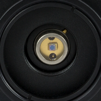
Click to Enlarge
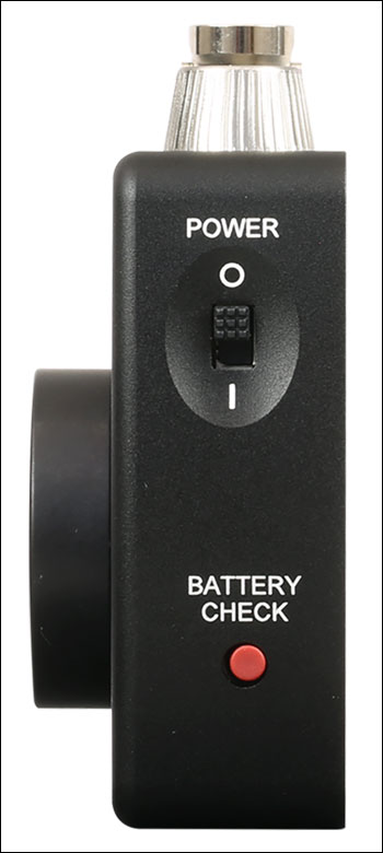
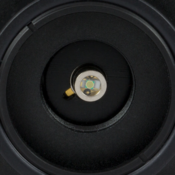
DET10D2の赤色のバッテリーテストボタン

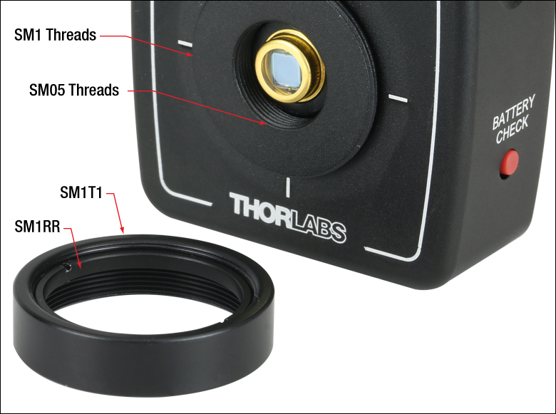
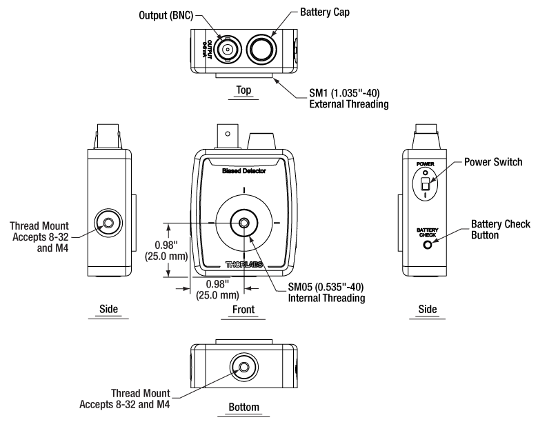
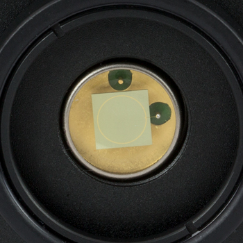
ディテクタのすべてのコネクタや操作スイッチ等は光路から離れて配置されているので、光学系などへの組み込みも容易です。各ディテクタにはSM05内ネジとSM1外ネジが付いています。 DETシリーズの筐体には取り外し可能なSM1カプラ(SM1T1)が付属しており、Ø25 mm~Ø25.4 mm(Ø1インチ) の光学フィルタやレンズなどの光学部品を光軸に沿って取り付けることができます。DETシリーズのディテクタは、ケージシステム、レンズチューブシステム、Ø12 mmまたはØ12.7 mmポストに取り付けることが可能です。 すべてのユニットの筐体にはM4ならびに#8-32ネジのどちらにも対応する取付け穴が2つ付いています。取り付け位置や取り付け方法については「筐体の特長」タブをご覧ください。
DETシリーズには、12 VDCのバッテリA23が内蔵されています。 筐体には、赤いバッテリーテストボタン(左図参照)が付いています。このボタンを押すと、外部負荷全体にバッテリの電圧が加えられます。 高いZ負荷に対しては、このボタンを押すことによってBNC経由でバッテリの電圧がBNCを通じて出力され、バッテリを取り外すことなく、交換時期にあるかどうかを判断することができます。インラインの電流制限抵抗によって、50 Ωの負荷抵抗器に接続したままバッテリの試験を行っても、すぐに損傷を与えることはありません。 メーカによって正極にわずかに物理的なバラツキがありますので、当社のDETシリーズ フォトディテクタにはEnergizer®のバッテリの使用をお勧めしています。 バッテリは低ノイズな電源なので、逆バイアス印加に使用されています。 バッテリの寿命が問題となる用途では、バッテリの代わりに電源アダプターキットDET2Bをご使用いただくことができます。追加の電池およびDET2Bは下記にご用意しております。
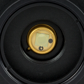
なお、ディテクタの検出部のエッジ部分の不均一性により、不要な静電容量や抵抗が生じることがあり、その結果、フォトダイオードからの出力に対する時間ドメインの応答が歪む場合があるので、その点にはご注意ください。 このような現象を防ぐためにも、フォトダイオードへの光が検出部の中心にしっかりと入射するように調整いただくことをお勧めしています。 筐体のSM1ネジにより、検出素子の前に、Ø25.4 mm(Ø1インチ)集光レンズやピンホールを取り付けることができます。
また、波長400~1700 nm用の自由空間光用高速ディテクタおよび高速光ファイバ用ディテクタもご用意しています。
Click to Enlarge
すべてのディテクタの筐体には赤いバッテリーチェック用のボタンが付いています。こちらの写真はDET10D2です。
Click to Enlarge
各ディテクタにはSM05内ネジとSM1外ネジが付いており、SM1内ネジ付きアダプタSM1T1と固定リングSM1RRが付属しています。
DETシリーズの筐体の特長
当社の高速ディテクタは薄型の設計です。 各筐体にはSM05内ネジとSM1外ネジが付いています。 また、右の写真のようにSM1内ネジ付きアダプタSM1T1と固定リングSM1RRが付属しています。SM1T1は厚さ2.8 mmまでの光学素子を保持できます。各ディテクタは下の写真のようにØ12 mmまたは12.7 mmポストを使用した取り付けが可能です。各ディテクタは、検出面が筐体の前面と同一平面にある設計のため、オプトメカニクスシステム内でのアライメントが容易になります。こちらにはM4ならびに#8-32ネジの両方が取り付け可能な取付穴も2つ付いております。利便性のために、背面パネルにはフォトダイオードの応答曲線が刻印されています。
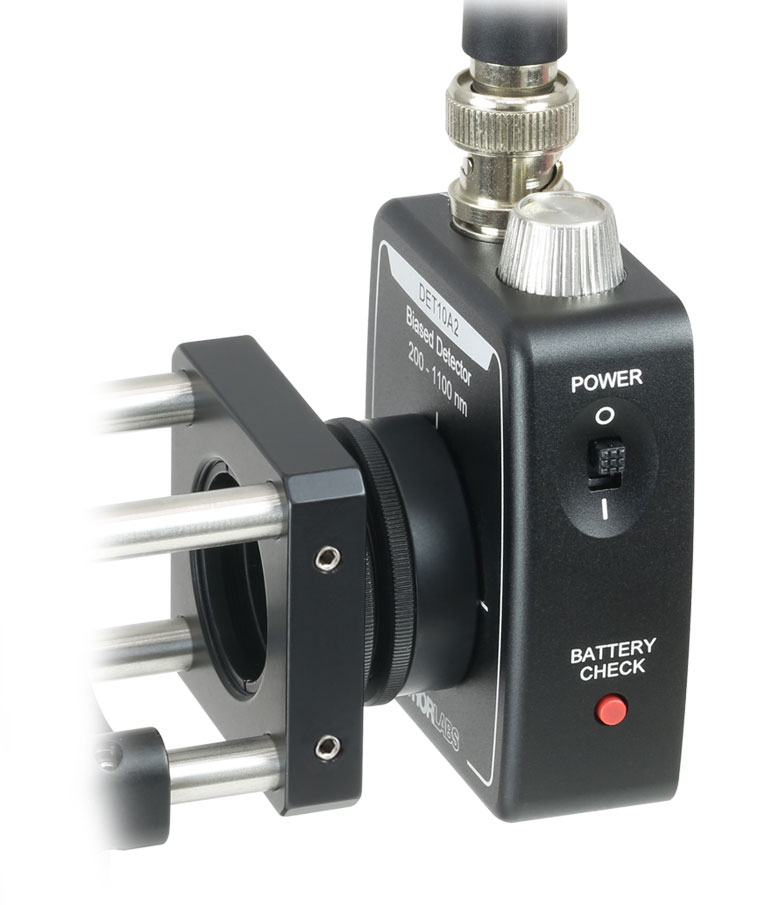
レンズチューブの取り付けについて
こちらのディテクタはSM05内ネジとSM1外ネジを使用して様々なオプトメカニクスシステムに組み込みが可能です。SM1ネジにレンズチューブを直接取り付けられるため、レンズチューブシステムにも対応します。アダプタSM1T1を使用して光学フィルタやレンズなどØ25 mm~Ø25.4 mm(Ø1インチ)の光学部品が取り付けられます。
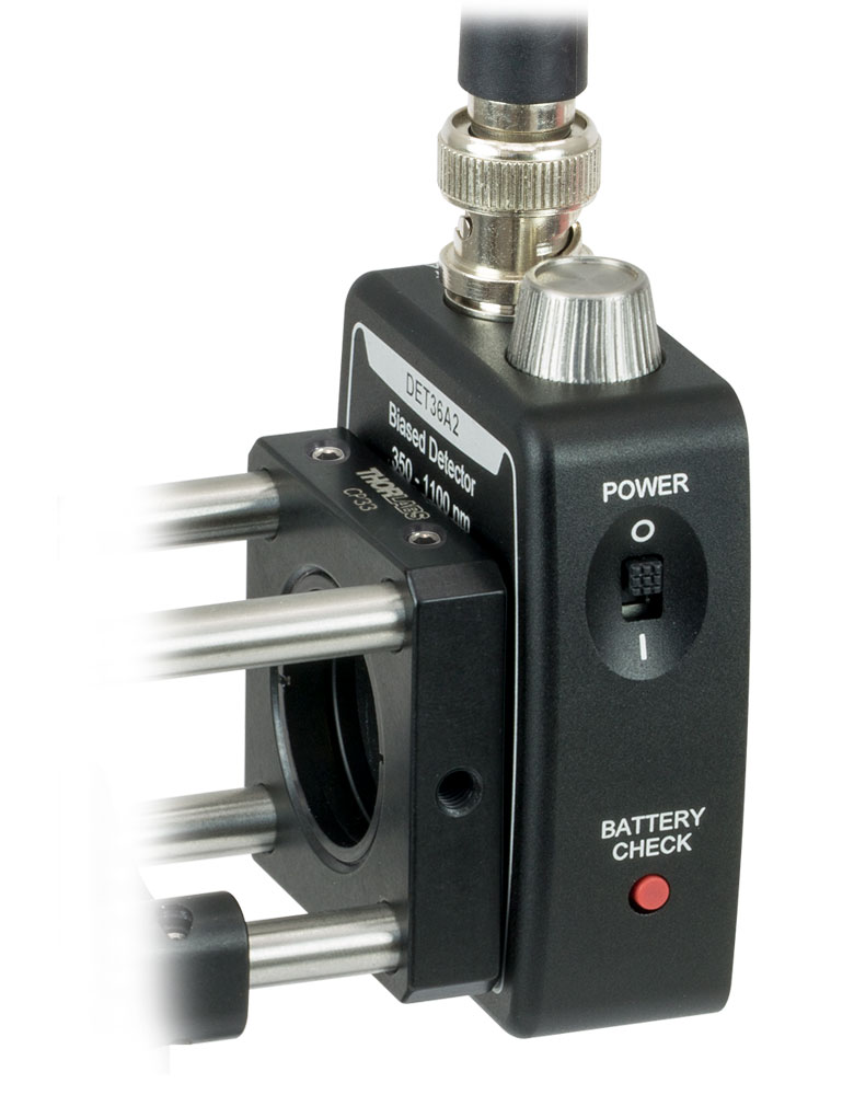
ケージシステムの取り付けについて
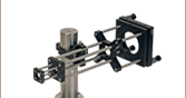
ディテクタは下記の2つの写真でご覧いただけるとおり、ケージシステムにも取り付けが可能です。ケージプレートCP33/Mは直接SM1ネジに取り付けられます。この方法ではアダプタを使用する必要がなく、フォトダイオードをできるだけケージプレートの近くに配置できるという利点があります。この利点は光が発散する光学系では特に重要になります。ほかにも付属のSM1T1とアダプタSM1T2を使用してディテクタをケージシステムに組み込む方法があります。この方法ではディテクタの方向の自由度が増します。またこちらのディテクタはSM1ネジ付きファイバーアダプタもご使用いただけます(下記参照)。
ポストの取り付けについて
ディテクタ筐体の取付用ネジ穴を選択することで、ユニットは、Ø12 mmまたは12.7 mmポストを使用して水平方向にも垂直方向にも取り付けることができます。 そのため、電源ケーブルとBNCケーブルを上から、もしくは光路の横に接続することが可能です。
Click to Enlarge
DETフォトディテクタを水平方向に取り付け

Click to Enlarge
DETフォトディテクタを30 mmケージシステム内のSM1レンズチューブに接続
Click to Enlarge
DETフォトディテクタをSM1外ネジで30 mmケージシステムに接続
| Housing Drawing (Click Icon for Details) | Mounting Taps | SM Thread Compatibility | Dimensions | Output Connector |
|---|---|---|---|---|
 | Two Universal Taps for 8-32 and M4 | Internal SM05 (0.535"-40)a External SM1 (1.035"-40) | 1.96" x 0.89" x 2.79" (49.8 mm x 22.5 mm x 70.9 mm) | BNC |
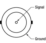
出力信号(光電流)
BNCメス型
各ディテクタのBNC出力端には50 Ωの終端抵抗器(例:型番T4119)を接続することをお勧めいたします。
光電流の最大値は下表の「Housing Features」をご覧ください。
注:旧世代の自由空間バイアスディテクタの仕様では最大出力電圧を記載していましたが、出力される信号は光電流でした。
混乱を避けるために新ディテクタについては出力電流を記載しています。ご迷惑をおかけしましたことをお詫び申し上げます。
電池の寿命
電池駆動のフォトディテクタを使う場合には、電池の寿命とそれがディテクタの駆動に与える影響を理解することが重要です。 電流出力デバイスとして、フォトディテクタの出力電流は、ディテクタに入射する光に比例します。 殆どの場合、終端抵抗を用いてこの電流を電圧へと変換します。 抵抗値は回路の利得とほぼ等しくなります。 DET08シリーズのような高速ディテクタでは、標準同軸ケーブルのインピーダンスを整合してケーブルの反射を減らし、全体的な信号の性能を向上させるために50 Ω終端抵抗を使うことが大切です。 多くの広帯域オシロスコープには、この終端抵抗が装備されています。
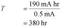
電池の使用寿命は、ディテクタによって使われる電流に直接関連します。 多くの電池製造メーカは、mAhで電池寿命を示しています。 例えば、ディテクタに付属の電池を190 mA hrsとして、これは、1.0 mAの電流で190時間動作します。 この電池を例として用い、以下に使用方法による電池寿命の算定方法について説明します。
この例では、平均光出力1 mWで波長780 nmの光源をディテクタに入力しています。 この波長での感度曲線に基づいたバイアス型フォトディテクタの感度は、0.5 A/Wとなります。光電流は次のように計算されます。
![]()
電池の定格寿命が190 mA hrの場合、電池の寿命は次のようになります。
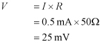
あるいは、16日の連続使用となります。 平均入射光を10 µWまで減らすと、同じ電池は連続使用で約4年間もちます。 推奨されている50 Ω終端抵抗を使うと、光電流0.5 mAは次の電圧に変換されます。
入射パワーレベルを40 µWまで減らすと、出力電圧は1 mVになります。 いくつかの測定装置では、この信号レベルは低すぎるので、電池寿命と測定確度の間で妥協を行なう必要があります。
バイアス型フォトディテクタを電池で駆動する場合、最小電圧レベルが必要であることを念頭において、できるだけ低い光強度を使うことが望ましいです。 また、電池は寿命が近付いても、すぐに電流が止まるわけではありません。 その代わり、電池の電圧が下がり、そして、フォトダイオードに印加されている電圧は減少します。 これにより、ディテクタの応答時間が長くなります(ディテクタの帯域幅が小さくなります)。 従って、ディテクタを特定のパラメータ内で動作させるために、電池が十分な電圧を有していることが重要です(ディテクタのマニュアル内「Troubleshooting」の章をご参照ください)。 電圧は、マルチメータを用いて確認することができます。
また、センサに入射している光を取り除いたり、出力を弱めたりすることでも電池の寿命は延びます。 光源がないと、フォトディテクタは暗電流に比例した電流を消費しますが、この電流は微小です。
DETシリーズのフォトダイオードが連続して比較的高パワーの光を照射される場合や電池を変えられない場合、アダプタDET2Bと電源(下記参照)をお使いください。 このオプションの欠点は、AC電源電圧の雑音が出力信号の雑音に加わり、測定がより不確かになる可能性がある点です。
フォトダイオードのチュートリアル
動作原理
接合型フォトダイオードは、通常の信号ダイオードと似た動作をする部品ですが、接合半導体の空乏層が光を吸収すると、光電流を生成する性質があります。フォトダイオードは、高速なリニアデバイスで、高い量子効率を達成し、様々な用途で利用することが可能です。
入射光の強度に応じた、出力電流レベルと受光感度を正確に把握することが必要とされます。Figure 100Aは、接合型フォトダイオードのモデル図で、基本的な部品要素が図示されており、フォトダイオードの動作原理が説明されています。
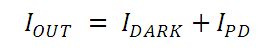
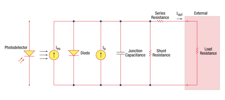
Figure 100A フォトダイオードの概略図
フォトダイオード関連用語
受光感度
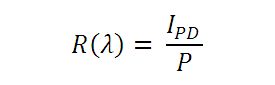
フォトダイオードの受光感度は、規定の波長における、生成光電流 (IPD)と入射光パワー(P)の比であると定義できます。
Photoconductiveモード(光導電モード)とPhotovoltaicモード(光起電力モード)
フォトダイオードは、Photoconductiveモード(逆バイアス) またはPhotovoltaicモード(ゼロバイアス)で動作できます。 モードの選択は、使用用途で求められる速度と、許容される暗電流(漏れ電流)の量で決まります。
Photoconductiveモード(光導電モード)
Photoconductiveモードでは、逆バイアスが印加されますが、これが当社のDETシリーズディテクタの基本です。回路で測定できる電流量はフォトダイオードに照射される光の量を反映します。つまり、測定される出力電流は、入射される光パワーに対しリニアに比例します。逆バイアスを印加すると、空乏層を広げて反応領域が広くなるため、接合容量が小さくなり、良好な線形応答が得られます。このような動作条件下では、暗電流が大きくなりがちですが、フォトダイオードの種類を選ぶことで、暗電流を低減することもできます。(注:当社のDETディテクタは逆バイアスで、順方向バイアスでは動作できません。)
Photovoltaicモード(光起電力モード)
Photovoltaicモードでは、フォトダイオードはゼロバイアスで使用されます。デバイスからの電流の流れが制限されると電位が上昇します。このモードでは光起電力効果が引き起こされますが、これが太陽電池の基本です。Photovoltaicモードでは、暗電流は小さくなります。
暗電流
暗電流とは、フォトダイオードにバイアス電圧が付加されている時に流れる漏れ電流です。Photoconductiveモードで使用する場合に暗電流の値は高くなりがちで、温度の影響も受けます。 暗電流は、温度が10°C上昇するごとに約2倍となり、シャント抵抗は6°C の上昇に伴い倍になります。高いバイアスを付加すれば、接合容量は小さくなりますが、暗電流の量は増大してしまいます。
暗電流の量はフォトダイオードの材料や検出部の寸法によっても左右されます。ゲルマニウム製のデバイスでは暗電流は高くなり、それと比較するとシリコン製のデバイスは一般的には低い暗電流となります。Table 100Bではいくつかのフォトダイオードに使用される材料の暗電流の量と共に、速度、感度とコストを比較しています。
| Table 100B Photodiode Materials | ||||
|---|---|---|---|---|
| Material | Dark Current | Speed | Spectral Range | Cost |
| Silicon (Si) | Low | High Speed | Visible to NIR | Low |
| Black Silicon (B-Si) | Low | Medium Speeda | Visible to NIR | Moderate |
| Germanium (Ge) | High | Low Speed | NIR | Low |
| Indium Gallium Arsenide (InGaAs) | Low | High Speed | NIR | Moderate |
| Indium Arsenide Antimonide (InAsSb) | High | Low Speed | NIR to MIR | High |
| Extended Range Indium Gallium Arsenide (InGaAs) | High | High Speed | NIR | High |
| Mercury Cadmium Telluride (MCT, HgCdTe) | High | Low Speed | NIR to MIR | High |
接合容量
接合容量(Cj)は、フォトダイオードの帯域幅と応答特性に大きな影響を与えるので、フォトダイオードの重要な特性となります。ダイオードの面積が大きいと、接合容量が大きくなり、電荷容量は大きくなります。逆バイアスの用途では、接合部の空乏層が大きくなるので、接合容量が小さくなり、応答速度が速くなります。
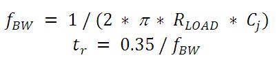
帯域幅と応答性
負荷抵抗とフォトディテクタの接合容量により帯域幅が制限されます。最善の周波数応答を得るには、50 Ωの終端装置を50 Ωの同軸ケーブルと併用します。接合容量(Cj)と負荷抵抗値(RLOAD)により、帯域幅(fBW)と立ち上がり時間応答(tr)の概算値が得られます。
雑音等価電力
雑音等価電力(NEP:Noise Equivalent Power)とは、出力帯域幅1 Hzでの信号対雑音比(SNR)が1になる入力信号のパワーです。NEPによって、ディテクタが低レベルの光を検知する能力を知ることができるので、この数値は便利です。一般には、NEPはディテクタの検出部の面積増加に伴って大きくなり、下記の数式で求めることができます。
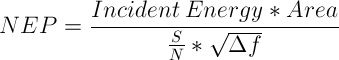
この数式において、S/Nは信号対雑音比、Δf はノイズの帯域幅で、入射エネルギ単位はW/cm2となっています。詳細は、当社のホワイトペーパー「NEP – Noise Equivalent Power」をご覧ください。
終端抵抗
オシロスコープでの測定を可能にするためには、生成された光電流を電圧(VOUT)に変換する必要がありますが、負荷抵抗を用いて電圧変換します。
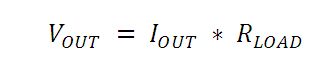
フォトダイオードの種類によっては、負荷抵抗が応答速度に影響を与える場合があります。最大帯域幅を得るには、50 Ωの同軸ケーブルを使用して、ケーブルの反対側の終端部で50 Ωの終端抵抗器の使用を推奨しています。このようにすることで、ケーブルの特性インピーダンスとマッチングできて共鳴が最小化できます。帯域幅が重要ではない特性の場合は、RLOADを増大させることで、所定の光レベルに対して電圧を大きくすることができます。終端部が不整合の場合、同軸ケーブルの長さが応答特性に対して大きな影響を与えます。したがってケーブルはできるだけ短くしておくことが推奨されます。
シャント抵抗
シャント抵抗は、ゼロバイアスフォトダイオード接合の抵抗を表します。理想的なフォトダイオードでは、シャント抵抗は無限大となりますが、実際の数値はフォトダイオードの材料の種類によって、10Ωのレベルから 数千MΩの範囲となる場合があります。例えばInGaAsディテクタのシャント抵抗は、10 MΩのレベルですが、GeディテクタはkΩのレベルです。このことは、フォトダイオードのノイズ電流に大きく影響を与える可能性があります。しかしながらほとんどの用途では、ある程度高い抵抗値であればその影響は小さく、無視できる程度です。
直列抵抗
直列抵抗は半導体材料の抵抗値で、この低い抵抗値は、通常は無視できる程度です。直列抵抗は、フォトダイオードの接触接続部とワイヤ接続部で発生し、ゼロバイアスの条件下でのフォトダイオードのリニアリティの主な決定要因になります。
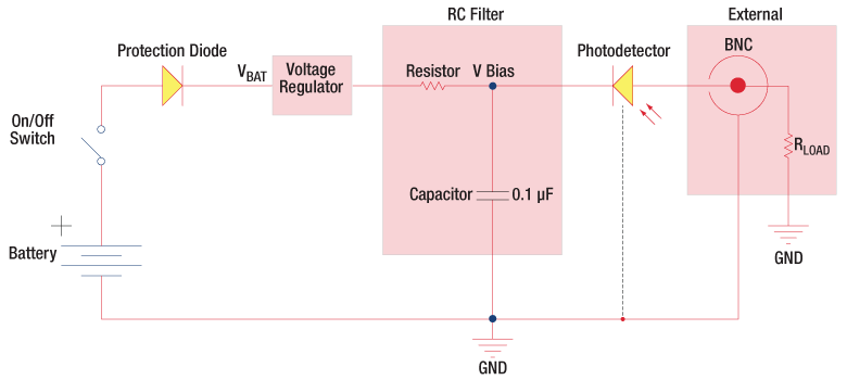
一般的な動作回路
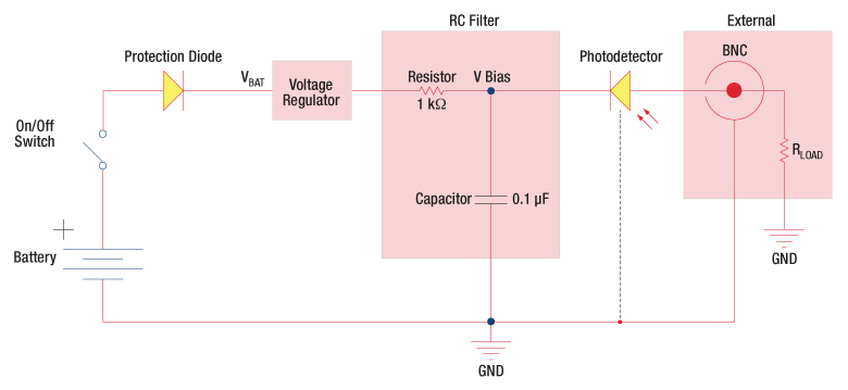
Figure 100C 逆バイアス回路(DETシリーズディテクタ)
Figure 100Cの回路はDETシリーズのディテクタをモデル化したものです。ディテクタは、入射光に対して線形の応答を得るために逆バイアス状態になっています。ここで生成された光電流の量は、入射光と波長に依存し、負荷抵抗を出力端子に接続すると、オシロスコープでモニタリングできます。RCフィルタの機能は、出力に雑音を載せてしまう可能性のある供給電力からの高周波雑音のフィルタリングです。

Figure 100D 増幅ディテクタ回路
高利得用途でアンプとともにフォトディテクタを使用できます。動作時には、PhotovoltaicモードまたはPhotoconductiveモードのいずれも選択可能です。このアクティブ回路はいくつかの利点があります。
- Photovoltaicモード:オペアンプで、点Aと点Bの電位が同じに維持されているので、フォトダイオードでは回路全体では0 Vに保たれています。このことで暗電流は発生しなくなります。
- Photoconductiveモード: フォトダイオードは逆バイアス状態であるので、接合容量を低下させ、帯域幅の状態を改善します。ディテクタの利得は、フィードバック素子(Rf)に依存します。ディテクタの帯域幅は、下記の数式で計算することができます。
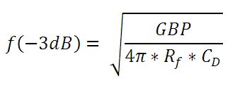
GBPが利得帯域幅積で、CDは接合容量と増幅器の静電容量の和です。
チョッパ入力周波数の影響
光導電信号は時定数の応答限界までは一定となりますが、PbS、 PbSe、HgCdTe (MCT)、InAsSbなどのディテクタにおいては、1/fゆらぎ(チョッパ入力周波数が大きいほどゆらぎは小さくなる)を持つため、低い周波数の入力の場合は影響が大きくなります。
低いチョッパ入力周波数の場合は、ディテクタの受光感度は小さくなります。周波数応答や検出性能は下記の条件の場合において最大となります。
![]()
暗電流の温度特性と逆バイアス電圧特性
いくつかの筐体付きディテクタについて、暗電流の温度特性と、逆バイアス電圧特性を測定しました。暗電流とは、以下に説明するように光が入射していないときのpn接合型フォトディテクタに流れる比較的小さい電流です。しかし用途によっては、温度の変動や逆バイアス電圧の変化による暗電流の変化を考慮しなければならない場合があります。バッテリをフォトダイオードの逆バイアス電圧用に使用した場合、バッテリが消耗するにつれて供給電圧が下がっていくため、逆バイアス電圧と暗電流の関係はとりわけ重要な場合があります。
最初の実験では、シリコン(Si)、ゲルマニウム(Ge)、そしてインジウムガリウムヒ素(InGaAs)のバイアス型フォトダイオードについて、温度を10 °C~50 °Cで変化させて測定しました。次の実験では、同じディテクタを24 °Cに保ちながら、逆バイアス電圧を0~10 Vで変化させて測定しました。実験や測定の詳細については下記のMore [+]をクリックしてご覧ください。
pn接合型フォトダイオードの電流-電圧特性
pn接合型フォトダイオードの電流-電圧特性は、順方向バイアスと逆方向バイアスの電圧でそれぞれ特徴があります。pn接合型フォトダイオードを動作させるときは逆バイアス電圧の領域で使用します。その場合、電圧はダイオードの順方向とは逆にかかります。筐体付きフォトダイオードの利便性の1つに、パッケージに内蔵されたバッテリにより逆バイアス電圧を供給できることがあります。逆バイアス型フォトダイオードに対して光が入射していないときには、電流が流れないのが理想です。
しかし実際にはフォトダイオードの半導体材料内部でのランダムプロセスにより、常に電流キャリア(電子と正孔)が生成され、それにより電流が発生します。このような電流の発生プロセスは、電子と正孔の光生成によるものではありません。それらの多くは半導体材料内部の熱エネルギによって発生します[1]。この暗電流は一般には小さいですが、フォトダイオードに逆バイアスをかけ、かつ光が照射されていない状態でも存在します。暗電流の大きさはフォトダイオードの素材構成によって異なり、熱的なプロセスによる発生効率はディテクタのセンサーヘッドに使用される半導体の種類と結晶品質に依存します。暗電流は、フォトダイオードの温度上昇と、フォトダイオードに印加される逆バイアス電圧の増加に伴い、大きくなることが予測されます。
注意しなくてはならないのは、逆バイアス電圧がある閾値を超えるとフォトダイオードは降伏し、急激に大きい電流が流れてダイオードが恒久的に損傷する可能性があることです。この理由により当社のDETパッケージの多くには、バイアス電圧が閾値を超えるのを防ぐ電圧レギュレータが付属しています。
フォトダイオードに光が照射されると、入射光により発生した電流(光電流)が暗電流に重畳されます。光電流のキャリアは入射光子のエネルギによって生成されます。照射される光の強度がある閾値を超えると、光電流は暗電流よりも大きくなります。光電流が暗電流よりも大きい場合には、光電流の大きさは全電流を測定した後、暗電流を差し引くことによって求められます。一方、光電流が暗電流より小さい場合には、その検出は不可能です。そのため、フォトダイオードの暗電流は最小化するのが望ましいことになります。
[1] J. Liu, Photonic Devices. Cambridge University Press, Cambridge, UK, 2005
| 暗電流の温度特性 |
|---|
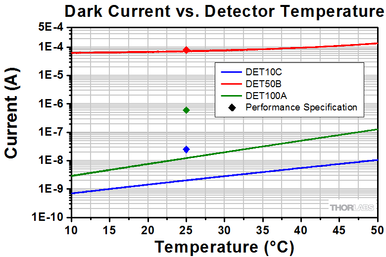
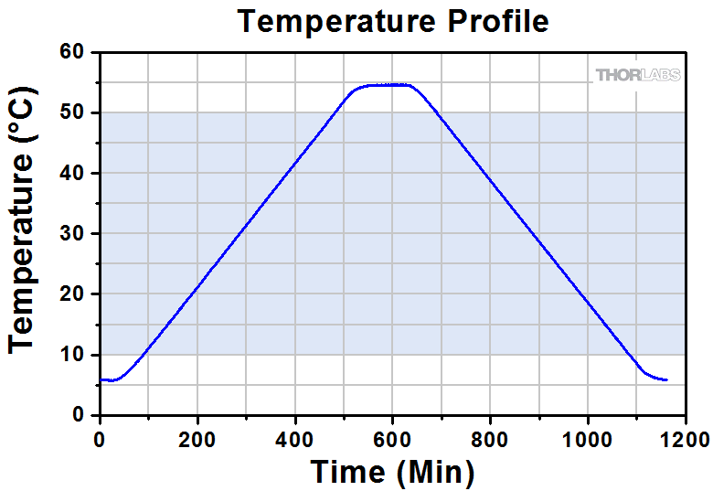
3つの代表的な筐体付きディテクタ(SiディテクタDET100A(旧製品)、GeディテクタDET50B(旧製品)、InGaAsディテクタDET10C(旧製品))について、その暗電流を10 °C~50 °Cの温度範囲で測定しました。 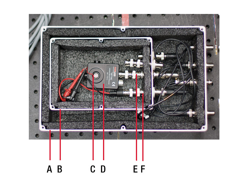 Click to Enlarge 図1: カバーを外し、DET10Cを設置した入れ子式金属ボックスの試験冶具。 どちらの箱も内側は黒色の断熱材で覆われています。 A: 外側のアルミニウム製ボックス、B:内側のアルミニウム製ボックス、C:サーミスタ、D: DET10C、E:BNC-Triaxフィードスルー、F:BNC-BNCフィードスルー。 実験のセットアップ 暗電流は逆バイアス電圧の大きさに依存するため、各測定期間中は逆バイアス電圧を一定に維持するようにしました。ディテクタの逆バイアス電圧源にはバッテリを使用しました。各データセットを取得する前には、ディテクタのバッテリA23を新しいものに交換しました。各テストの前後でバッテリの電圧を測定し、測定中のバイアス電圧が一定であることを確認しています。 実験中のフォトダイオードの温度は、サーミスタを用いて連続的にモニタしました。サーミスタはTO can型パッケージの外面に接触させ、熱伝導テープで固定しました。サーミスタを付けたため、ダイオードへの光を遮断するのにディテクタのキャップを使用することはできませんでした。 ディテクタは2つの入れ子式アルミニウム製ボックスで囲っています(図1はカバーを外した状態です)。1つのボックスのみでフォトダイオードを遮光することはできますが、実験ではEMIノイズを遮断するためにその外側にもボックスを使用しています。 ディテクタは内側のボックス内に設置し、そのボックスにはBNC-Triaxフィードスルーアダプタが取り付けられています。BNC端子は箱の内側に、Triax端子は箱の外側に配置されています。ディテクタのBNCコネクタは直接アダプタのBNC端子に取り付けられるため、BNCケーブルは不要でした。BNCケーブルの遮蔽性能は低く、それを使用したときにはディテクタからの信号にEMI源からのノイズが混入する場合があります。内側の金属ボックスは外側の金属ボックス内に配置されていますが、この外側のボックスにはTriax-Triaxフィードスルーが付いています。ディテクタの信号が通る内側と外側のボックスのフィードスルー間にはTriaxケーブルで接続しました。 外側のボックスのTriax-Triaxフィードスルー端子とアンメータKeithly6487の接続にも、Triaxケーブルを用いました。外側の金属ボックスは内側のボックスへのEMIを遮断し、Triaxケーブルはディテクタ信号へのEMIを遮断しています。2つのボックスにそれぞれ蓋をした後、ボックスセット一式をESPEC温度チャンバESX-3CW内に設置しました。アンメータはチャンバの外に設置しました。 サーミスタと温度ロガーTSP01間の電気的接続にはBNCケーブルを使用し、BNC-BNCバルクヘッドフィードスルーで入れ子式ボックスの外へ信号を取り出し、カスタム仕様のBNC-フォノジャックケーブルを使用して温度ロガーに接続しました。 実験結果 図2からは、暗電流はGeディテクタが最大であることのほかに、どのフォトダイオードも予測した通り温度が上昇すると暗電流も増加していることが分かります。どのフォトダイオードも、予測した通り温度が上昇すると暗電流も増加しています。グラフのひし形の点は25 °Cでの各ディテクタの暗電流の仕様値です。これらの点は25 °Cでの暗電流の最大値を示しています。各ダイオードは25 °Cではこの値、もしくはそれよりも小さい値でなければなりませんが、25 °Cよりも高い温度ではディテクタDET50Bのようにこの仕様値よりも大きくなる場合があります。 実験結果についての制限事項 |
| 暗電流の逆バイアス電圧特性 |
|---|
3つの代表的な筐体付きディテクタ(SiディテクタDET100A(旧製品)、GeディテクタDET50B(旧製品)、InGaAsディテクタDET10C(旧製品))の温度を24 °Cに保ち、逆バイアス電圧を0~10 Vで変化させて暗電流を測定しました。逆バイアス電圧の供給にはバッテリ、もしくはパワーアダプタDET2Bのような外部電源を使用することができます。下の測定はバッテリの消耗に伴う供給電圧の低下とともに、暗電流がどのように変化するかを示す目的で行われました。 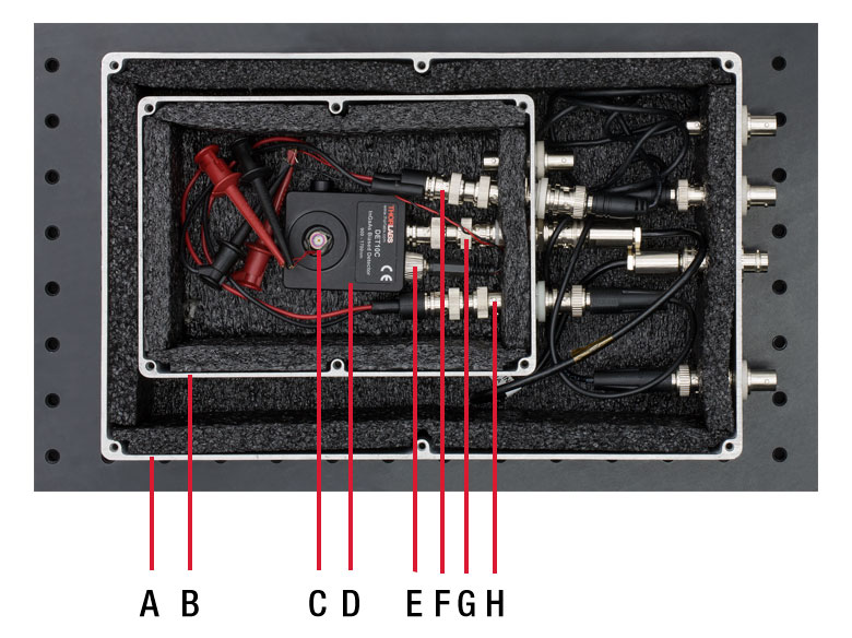 Click to Enlarge 図1: カバーを外し、DET10Cを設置した入れ子式金属ボックスの試験冶具。 どちらの箱も内側は黒色の断熱材で覆われています。 A: 外側のアルミニウム製ボックス、B:内側のアルミニウム製ボックス、C:サーミスタ、D: DET10C、E:電源DET1Bのパワーアダプタ、F:DET1B用BNC-BNCフィードスルー、 G:ディテクタの信号用BNC-Triaxフィードスルー、H:サーミスタ用BNC-BNCフィードスルー。 実験のセットアップ ディテクタは2つの入れ子式アルミニウム製ボックスで囲っています(図1はカバーを外した状態です)。1つのボックスのみでフォトダイオードを遮光することはできますが、実験ではEMIノイズを遮断するためにその外側にもボックスを使用しています。ディテクタは内側のボックスに入れ、BNCとBNC-Traixアダプターフィードスルーを使用して電気的に接続しました。 ディテクタからの測定信号はBNC-Traixアダプターフィードスルーを通ります。ディテクタのBNCコネクタは直接アダプタのBNC端子に取り付けられるため、BNCケーブルは不要でした。BNCケーブルの遮蔽性能は低く、それを使用したときにはディテクタからの信号にEMI源からのノイズが混入する場合があります。内側の金属ボックスは外側の金属ボックス内に配置されていますが、この外側のボックスにはTriax-Triaxフィードスルーが付いています。ディテクタの信号が通る内側と外側のボックスのフィードスルー間にはTriaxケーブルを使用しました。外側のボックスのTriax-Triaxフィードスルー端子とアンメータKeithly6487の接続にも、Triaxケーブルを用いました。外側の金属ボックスは内側のボックスへのEMIを遮断し、Triaxケーブルはディテクタ信号へのEMIを遮断しています。2つのボックスにそれぞれ蓋をした後、ボックスセット一式をESPEC温度チャンバESX-3CW内に設置しました。アンメータはチャンバの外に設置しました。 逆バイアス電圧は、DET1B(旧製品、現行品はDET2B)を使用してBNCフィードスルーを通じて供給しました。DET1Bは電源とDETシリーズディテクタのバッテリーポートに挿入するよう設計されたパワーアダプタから構成されています。パワーアダプタをディテクタに挿入し、もう一方のアダプタ端を内側ボックスの壁にはめられたBNCフィードスルーに接続しました。外側ボックスの外部までの電気的接続にはBNCケーブルともう1つのフィードスルーを使用し、Keithley 6487の電圧出力端子に接続しました。Keithley 6487をPCに接続することで、逆バイアス電圧を制御しながら同時に暗電流を測定することが可能でした。 暗電流は温度に大きく依存するため、実験中はサーミスタを使用して各フォトダイオードの温度を継続的にモニタしました。サーミスタはTO can型パッケージの外面に接触させ、熱伝導テープで固定しました。サーミスタを付けたため、ダイオードへの光を遮断するのにディテクタのキャップを使用することはできませんでした。サーミスタと温度ロガーTSP01間の電気的接続にはBNCケーブルを使用し、BNC-BNCバルクヘッドフィードスルーで入れ子式ボックスの外へ信号を取り出し、カスタム仕様のBNC-フォノジャックケーブルを使用して温度ロガーに接続しました。 実験結果 SiディテクタDET100Aには電圧レギュレータは内蔵されていませんが、GeディテクタDET50BとInGaAsディテクタDET10Cには内蔵されています。ディテクタ内蔵の電圧レギュレータは、フォトダイオードに印加される逆バイアス電圧を一定に保つ役割を果たします。 一般に、電圧レギュレータは安定な電圧レベルを自動的に維持するために、様々な用途で使用されています。その入力電圧が所定の範囲内であれば、出力電圧レベルはほぼ一定になるように制御されます。しかし入力電圧が、電圧レギュレータが正常に機能する電圧範囲の下限を下回ると、レギュレータは出力電圧を制御できなくなります。入力電圧がさらに下がり続けると出力電圧も下がり、ある閾値まで下がるとレギュレータは全く機能しなくなります。このオフ状態では、出力電圧は無視できるレベルになります。GeディテクタDET50BとInGaAsディテクタDET10Cの場合、電圧レギュレータの出力電圧がフォトダイオードの逆バイアスに使用されます。 SiディテクタDET100Aには電圧レギュレータが内蔵されていないため、測定された暗電流は図2のグラフの通り、Keithley 6487が供給する電圧の増加とともに増加し続けます。DET100Aで測定された暗電流は、0.5 Vの逆バイアス電圧までは指数関数的に増え、逆バイアス電圧が約0.5 V~10 Vの間は直線的に増加します。 新しいバッテリでは10 V以上の電圧が供給されます。 この閾値までの電圧は電圧レギュレータのオフ状態に相当します。電圧が閾値を超えると、Keithley 6487の供給する電圧が5.5 Vに達するまで、ディテクタの暗電流は増加します。供給電圧が5.5 V~10 Vの間では、電圧レギュレータがフォトダイオードに供給する逆バイアス電圧を一定に維持するため、この範囲における暗電流はおおよそ一定しています。 新しいバッテリでは10 V以上の電圧が供給されるため、電圧レギュレータはほぼバッテリの寿命が続く間、暗電流をほぼ一定に保つとともに、一般的にフォトダイオードに過剰な逆バイアス電圧がかからないよう保護する効果もあります。 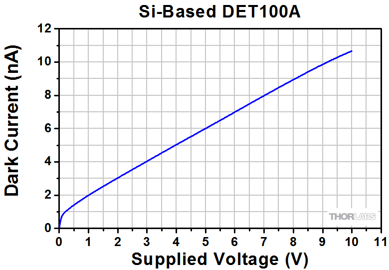 Click to Enlarge 図2: Siベースのパッケージ付きフォトダイオードDET100A(電圧レギュレータ無し)で測定された暗電流データをKeithley 6487から供給された電圧の関数としてグラフ化しています。 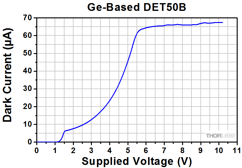 Click to Enlarge 図3: Geベースのパッケージ付きフォトダイオードDET50B(電圧レギュレータ内蔵)で測定された暗電流データをKeithley 6487から供給された電圧の関数としてグラフ化しています。 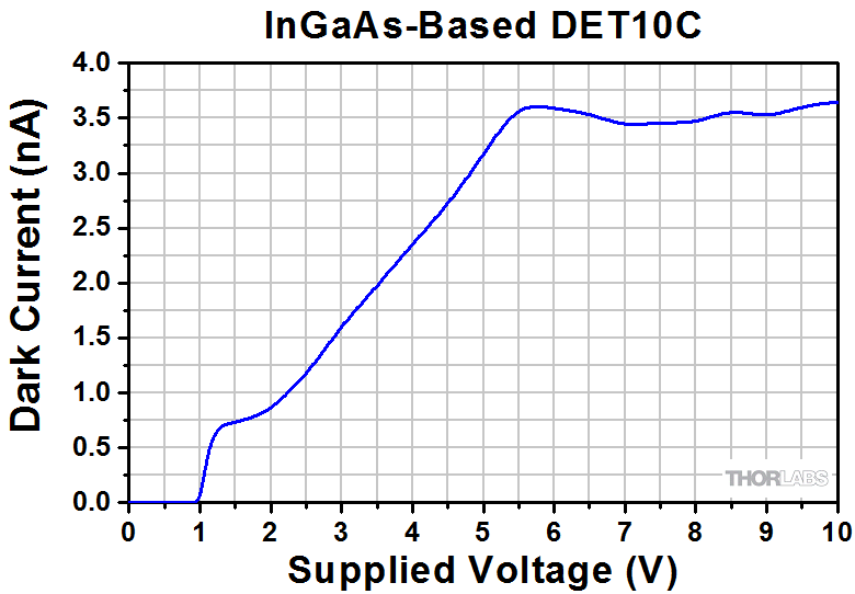 Click to Enlarge 図4: InGaAsベースのパッケージ付きフォトダイオードDET10C(電圧レギュレータ内蔵)で測定された暗電流データをKeithley 6487から供給された電圧の関数としてグラフ化しています。 実験結果についての制限事項 |
下表は当社のPDA、PDFならびにDETディテクタの旧製品と現製品の一覧です。
| Previous Generation Cross Reference of PDA and DET Detectors | |||||
|---|---|---|---|---|---|
| Wavelength | Material | Biased Detector | Amplified Detector | ||
| Current Generation | Previous Generation | Current Generation | Previous Generation | ||
| 200 - 1100 nm | Si | DET10A2 | DET10A(/M) | PDA10A2 | PDA10A(-EC) |
| 320 - 1000 nm | Si | - | - | PDA8A2 | PDA8A |
| 400 - 1000 nm | Si | - | - | PDA015A2 | PDA015A(/M) |
| 320 - 1100 nm | Si | DET100A2 | DET100A(/M)a | PDA100A2 | PDA100A(-EC)b |
| Si | - | - | PDF10A2 | PDF10A(/M) | |
| 350 - 1100 nm | Si | DET36A2 | DET36A(/M) | PDA36A2 | PDA36A(-EC) |
| 500 - 1700 nm | InGaAs | DET10N2 | DET10N(/M) | - | - |
| 800 - 1700 nm | InGaAs | DET20C2 | DET20C(/M) | PDA20CS2 | PDA20CS(-EC) |
| - | - | PDA05CF2 | PDA10CF(-EC) | ||
| - | - | PDA015C2 | PDA015C(/M) | ||
| - | - | PDF10C2 | PDF10C(/M) | ||
| - | - | PDA20C2 | PDA20C(/M) | ||
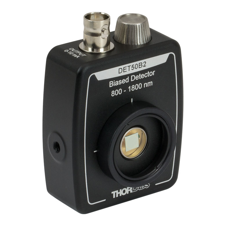
| 800 - 1800 nm | Ge | DET30B2 | DET30B(/M) | PDA30B2 | PDA30B(-EC) |
| DET50B2 | DET50B(/M) | PDA50B2 | PDA50B(-EC) | ||
| 900 - 1700 nm | InGaAs | DET10C2 | DET10C(/M) | PDA10CS2 | PDA10CS(-EC) |
| 900 - 2600 nm | InGaAs | DET05D2 | DET05D(/M)c | PDA10D2 | PDA10D(-EC)c |
| DET10D2 | DET10D(/M)c | - | - | ||
パルスレーザ:パワーとエネルギーの計算

パルスレーザからの放射光が、使用するデバイスや用途に適合するかどうかを判断する上で、レーザの製造元から提供されていないパラメータを参照しなければならない場合があります。このような場合、一般には入手可能な情報から必要なパラメータを算出することが可能です。次のような場合を含めて、必要な結果を得るには、ピークパルスパワー、平均パワー、パルスエネルギ、その他の関連するパラメータを必要とすることがあります。
- 生物試料を損傷させないように保護する
- フォトディテクタなどのセンサにダメージを与えることなくパルスレーザ光を測定する
- 物質内で蛍光や非線形効果を得るために励起を行う
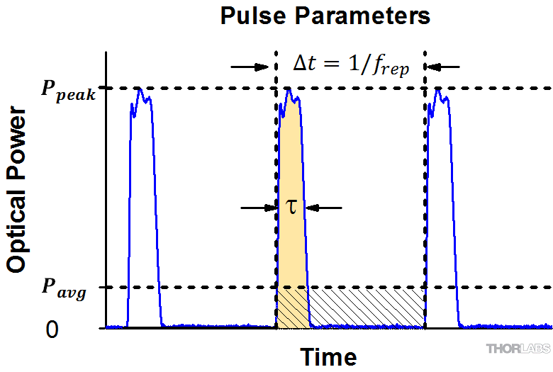
パルスレーザ光のパラメータは下の図1および表に示します。参照用として、計算式の一覧を以下に示します。資料を ダウンロードしていただくと、これらの計算式のほかに、パルスレーザ光の概要、異なるパラメータ間の関係性、および計算式の適用例がご覧いただけます。
計算式 | ||||
 | 、 |  | ||
 | ||||
 | ||||
 | ||||
平均パワーから算出するピークパワー、ピークパワーから算出する平均パワー : | ||||
 | 、 |  | ||
| 平均パワーおよびデューティーサイクルから算出するピークパワー*: | ||||
 | *デューティーサイクル( ) はレーザのパルス光が放射されている時間の割合です。 ) はレーザのパルス光が放射されている時間の割合です。 | |||
Click to Enlarge
図1: パルスレーザ光の特性を記述するためのパラメータを、上のグラフと下の表に示します。パルスエネルギ (E)は、パルス曲線の下側の黄色の領域の面積に対応します。このパルスエネルギは斜線で表された領域の面積とも一致します。
| パラメータ | シンボル | 単位 | 説明 | ||
|---|---|---|---|---|---|
| パルスエネルギ | E | ジュール[J] | レーザの1周期中に放射される1パルスの全放射エネルギ。 パルスエネルギはグラフの黄色の領域の面積に等しく、 これは斜線部分の面積とも一致します。 | ||
| 周期 | Δt | 秒 [s] | 1つのパルスの開始から次のパルスの開始までの時間 | ||
| 平均パワー | Pavg | ワット[W] | パルスとして放射されたエネルギが、1周期にわたって 均一に広がっていたと仮定したときの、 光パワーの大きさ(光パワー軸上の高さ) | ||
| 瞬時パワー | P | ワット[W] | 特定の時点における光パワー | ||
| ピークパワー | Ppeak | ワット [W] | レーザから出力される最大の瞬時パワー | ||
| パルス幅 |  | 秒 [s] | パルスの開始から終了までの時間。一般的にはパルス形状の 半値全幅(FWHM)を基準にしています。 パルス持続時間とも呼ばれます。 | ||
| 繰り返し周波数 | frep | ヘルツ [Hz] | パルス光が放射される頻度を周波数で表示した量。 周期とは逆数の関係です。 | ||
計算例
下記のパルスレーザ光を測定するのに、最大入力ピークパワーが75 mW
のディテクタを使用するのは安全かどうかを計算してみます。
- 平均パワー: 1 mW
- 繰り返し周波数: 85 MHz
- パルス幅: 10 fs
1パルスあたりのエネルギは、

と低いようですが、ピークパワーは、

となります。このピークパワーはディテクタの
最大入力ピークパワーよりも5桁ほど大きく、
従って、上記のパルスレーザ光を測定するのに
このディテクタを使用するのは安全ではありません。
| Posted Comments: | |
Heonsik Lee
(posted 2024-07-03 17:20:30.483) Hi,
I'm Heonsik Lee, from KAIST, Korea.
Is the output of 'DET100A2' a current or voltage?
I use the oscilloscope for measuring the voltage with T-connector with 50 ohm terminator, but no signal measured; rather, if I connect the PD-oscilloscope directly with a BNC cable, I can measure the voltage.
And, also I want to know the maximum output. the manual said maximum current is 10 mA, and maximum output is 9V(HI-Z), 170 mV(50 ohm). is it linearly related to min-max laser power? ksosnowski
(posted 2024-07-03 10:59:01.0) Hello Heonsik, thanks for reaching out to us. The DET series output photocurrent in response to applied light. The impedance of the measurement acts as a gain factor to voltage conversion so with 50 Ohm termination you see a fairly low 50 V/A. A higher impedance can be used for higher gain at a direct cost to the bandwidth of the detector. Your observation is very common for customers using a scope with a high input impedance. The maximum output current should be kept below 10mA to avoid damaging the microwires on the photodiode in any scenario. With high impedance though, you will experience saturation before reaching 10mA of photocurrent. Saturation will occur slightly above the bias level of the detector used and can cause the photodiode to degrade as photons can only convert to heat at this point, making the power measurement nonlinear as well. The 170mV you reference is in regards to the battery check function of the detector and is due to the current limiting resistor applied by the battery check button. Using an impedance much larger 2540 Ohm will allow you to read the entire battery voltage directly, and if only 9V can be measured though the battery check, we would consider the battery exhausted. Birgit Lange
(posted 2024-06-20 07:10:31.57) Sorry, but I could not find the maximum peak optical input power for the DET10D2.
Could you please give me this value (wavelength: 1940nm).
Thank you very much for your help!
Kind regards,
Birgit Lange ksosnowski
(posted 2024-06-25 06:04:08.0) Hello Birgit, thanks for reaching out to Thorlabs. The maximum power of the DET series is limited by either saturation or photocurrent limits depending on the situation. There is also more detail on this in the previous feedbacks. DET10D2's maximum photocurrent rating is 5mA, and by estimating the typical responsivity around 1940nm as 1.3A/W, this gives a practical upper limit of 3.85mW with 50 Ohm termination, or less with higher impedance values where one would experience saturation. If you consider a 1MOhm impedance measurement, then at 1000000 V/A, you would surpass the 1.8V bias of DET10D2 closer to 1.4uW. I have reached out directly to discuss this in further detail. Xianghe Wang
(posted 2024-05-02 22:28:15.937) 我想知道怎么查看每款型号的最大可探测功率 ksosnowski
(posted 2024-05-02 12:44:44.0) Hello Xianghe, thanks for reaching out to Thorlabs. The maximum power of the DET series is limited by either saturation or photocurrent limits depending on the situation. Saturation occurs relative to the detector's fixed bias voltage, so the optic power that leads to saturation also depends on the diode's spectral responsivity, and the measurement load used. High impedance measurements provide higher gain but it is easy to saturate at lower powers with the 1MOhm impedance common to oscilloscopes. 50 Ohm termination, as required for the full detector bandwidth, leads to a gain of 50 V/A, and in this case one typically will hit the max current output of the DET well before reaching saturation across the smaller load. Exceeding the photocurrent limits can burn out the microwires connecting the diode. We do not have a surface damage threshold for the photodiodes however this would be well past saturation if using at least 80% of the active area of these devices. As both these limits depend on the wavelength and measurement load of the application, we do not specify a single maximum optical power level directly. Your local tech support team has reached out to discuss this further. Echo Liang
(posted 2024-03-20 15:41:24.057) 您好,之前在thorlabs购买了DET100A/M产品想知道它的上升时间是多少。目前在网站上没有相关信息被DET100A2替代。 ksosnowski
(posted 2024-03-20 12:01:35.0) Hello Echo, thanks for reaching out to Thorlabs. DET100A used a slightly different diode than our current DET100A2 model. The device manual and specs can still be found by searching our site for DET100A. With a 50 Ohm load and fresh 12V A23 battery, the rise time is specified as 43ns. Above 800nm in large-area silicon detectors (10mm x 10mm, 3.6mm x 3.6mm) we have noted an increased rise time as you go deeper into the NIR range. A member from your local tech support team has reached out directly to discuss this further. Alexander Voronov
(posted 2024-01-11 16:21:49.237) Hi.
In our application the space is constrained, DET100A2 doesn't fit to it. Could you make a product similar to SM1PD1B(mount), but with the photodiode characteristics like DET100A2 (with externally provided bias)?
Thank you! ksosnowski
(posted 2024-01-11 10:26:50.0) Hello Alexander, thanks for reaching out to Thorlabs. We offer PBM42 bias module which can be connected via coax cable between the SM1PD1B and your measurement to apply an external bias, making a similar system to the DET series. We do also offer PDAPC2 which is an OEM style photodiode, bias, and amplifier circuit on a compact PCB for integration in systems like this. However, there isn't much space for pushing the bias RC filter and connection into the mounted photodiode housing itself. I have reached out directly to discuss this application further. Mirko Campo
(posted 2024-01-10 15:23:05.887) Dear Sir,
I have a DET10A2 detector. What is its maximum peak optical input power? Thank you for your attention. ksosnowski
(posted 2024-01-10 01:17:48.0) Hello Mirko, thanks for reaching out to us. DET10A2 has a 10mA max photocurrent limit so near the peak of responsivity 0.44 A/W this would be roughly 20mW. If using a larger load like 1MOhm, you may hit the 10V bias and saturation point at even lower photocurrent levels due to Ohm's law. A low battery will lower the bias and saturation point as well. If you are saturating the sensor, then use a lower load resistance or less optic power to keep the response linear. Saturation causes the sensor to degrade ultimately resulting in an increased dark device current. mark d
(posted 2023-06-13 11:29:39.743) This detector, DET36A2, and others we have from Thorlabs, has a "battery check" button, but I have found no instructions how to use it. I push it, but nothing seems to change. How is it supposed to work? ksosnowski
(posted 2023-06-13 01:00:49.0) Hello Mark, thanks for reaching out to Thorlabs. Page 7 of the DET36A2 manual covers the setup for battery measurements to check the bias. We recommend measuring the battery with a high impedance device. Many oscilloscopes have a HiZ setting and/or channel for this. As covered in the manual, using small loads will effect the measurement due to the current limiting resistor in the DET36A2. A low battery will result in reduced bandwidth and a lower saturation point. I have reached out directly to discuss this further. Robert McCoy
(posted 2023-06-12 12:33:01.31) Greetings,
Can you tell me what photodiode is used in the Det100A2 biased SI detector?
Thanks and regards,
Bob ksosnowski
(posted 2023-06-13 01:03:12.0) Hello Robert, thanks for reaching out to Thorlabs. Unfortunately the exact photodiode used in DET100A2/PDA100A2 is considered proprietary. However our closest bare photodiode is the silicon-based FDS1010. I have reached out directly to discuss your application in more detail. Yutong Feng
(posted 2023-03-30 10:47:48.087) Hello,
I have a DET10C2 and its output current is 0-5mA. I use a 50 ohm BNC cable to connect the detector and oscilloscope. The oscilloscope is set to DC50 ohm coupling. In this configuration, is 250 mV the maximum voltage reading on the scope before the DET10C2
is saturated?
Thank you. ksosnowski
(posted 2023-04-03 01:43:37.0) Hello Yutong, thanks for reaching out to Thorlabs. This max current rating is due not to saturation but limits on the wire bonds of the photodiode. Exceeding this level of photocurrent can result in device failure directly. Ohm's law will determine the voltage this occurs at based on your load resistance. Saturation will occur at a voltage equal to the bias; 5V for DET10C2. In practice, with 50 Ohm you will hit the photocurrent limit before reaching saturation voltage. With higher loads, saturation will occur with less photocurrent due to Ohm's law. We generally do not specify an optical saturation point directly since it varies with load and wavelength. Please note the DET series battery check feature can produce up to 10V in HiZ as noted in the DET manual. Alberto Hohenzollern
(posted 2023-03-21 08:39:16.047) Hello, we would like to use the photodetector DET20X2 for 850 nm photodetection requiring high saturation power (> 3 mW), low noise and low bandwidth (3 - 5 MHz would be sufficient). We were thinking of using a relatively high load resistor at the output ( 500 Ohm - 5 kOhm) to reduce the Johnson NEP, but we are not sure about the bandwidth that we could achieve in our scenario. From the manual, it seems like the dominant term for limiting the bandwidth is the sheet resistance, but it is not clear what the diffusion time constant would be at 850 nm. Could you provide some rough numbers clarifying the bandwidth of the photodetector at 850 nm? Thanks! ksosnowski
(posted 2023-04-25 11:54:28.0) Hello Alberto, thanks for reaching out to Thorlabs. The sheet resistance and diffusion time constant are dominating terms for bandwidth over the NIR range of this detector. The DET20X2 manual's bandwidth section covers this effect and equations to model in greater detail. These effects start around 800nm, and while we have not yet fully swept the upper wavelengths to poll bandwidth, we do have some limited data in this range to share. I have reached out directly to discuss this in further detail. Daniel Aponte
(posted 2023-01-18 11:40:41.107) Hi, I am using a DET10A2 to test a Shutter (AOM) with a UV laser 365nm WL. What we see is a very hi oscillating signal on the Oscilloscope. I wonder if you have a way to test.
If have a graph reference to WL and V-out or any other data can be used to. ksosnowski
(posted 2023-01-25 01:59:18.0) Thanks for reaching out to Thorlabs. The DET10A2 manual, page 13, has the Spectral Responsivity in A/W across the wavelength range of this detector. This can be used to relate the photocurrent to the input light level. Ambient lights can couple to the sensor if it is not shielded, and often result in a 60Hz signal which matches the mains frequency. Page 7 has the equation for bandwidth and rise time, which will depend on the load resistance and diode capacitance (i.e. bias); as well as the output voltage equation, which also depends on load resistance, and generated photocurrent from the sensor. Roger Putnam
(posted 2022-09-22 13:38:06.563) Greetings,
Can you send a graph of the pulse response of DET36A2 (actually want it for obsolete DET36A). Specifically we're interested in the turn-off behavior, both the speed of turn-off, and especially the slow (low) tail that is unfortunately common in fast detectors.
Question 2: Is the slow, low tail in the detector turn-off badly affected if too much light intensity is used on the detector?
Thanks,
Roger ksosnowski
(posted 2022-09-29 02:49:42.0) Thanks for reaching out to Thorlabs. We do not have an exact impulse response plot for the DET36A/A2 models, however we verify the rise time directly on these units in production. These use the FDS100 photodiode which we expect to have a similar rise and fall time. Other diodes like FDS015 have a much longer fall time than their rise. Saturating the detectors can negatively effect the bandwidth and rise/fall time of the detectors by increasing the effective resistance. I have reached out directly to discuss this further. Jaden Lee
(posted 2022-07-28 14:42:48.247) In specifications(DET10A2), the rise time means data acquisition rate?
for example, the DET10A2' rise time is 1 ns
1ns = 1e-9 sec => 10e9 hz = 1000000 khz = 1000 mhz
the DET10A2' data acquisition rate is 1000 mhz ? ksosnowski
(posted 2022-07-28 04:43:26.0) Thanks for reaching out to Thorlabs. Our detectors output an analog signal continuously. The measured rise time describes how long it takes for the active area to respond to an input optical signal and charge up from ~0V. This is due to capacitance and resistance in the photodiode and measurement system. Biased Photodiodes lower this capacitance for a faster response. A lack of bias voltage, or extra system capacitance i.e. due to cabling can negatively effect the response time and bandwidth. The bandwidth for each unit is calculated for an analog sine wave, for other waveforms it will be lower. Square waves for example will take roughly 10x the bandwidth of a sine wave at same frequency to preserve definition. Anton Ryzhov
(posted 2022-05-17 15:51:45.58) Dear Thorlabs team,
why has DET25K2 been discontinued? I do not see an adequate substitution in your actual DET-range... ksosnowski
(posted 2022-05-23 12:31:47.0) Unfortunately we had to discontinue all of our GaP based sensors as this type of diode is no longer being produced. Currently we do not have a direct alternative for this UV performance however we are hoping to replace this with a UV-enhanced Silicon based sensor in the future. We aim to cover a similar UV wavelength range while maintaining device performance. We do not yet have a timeline for this new product. Mark Johnston
(posted 2021-07-12 15:35:34.73) What is the window material on the DET10A2 detector? Can you get one without a window? Thanks. YLohia
(posted 2021-07-13 08:53:32.0) Hello, the window is made of Quartz, nominally 0.5 mm thick. Custom items can be requested by emailing techsales@thorlabs.com. We will discuss the possibility of offering a version of this without the window directly. Mark Johnston
(posted 2021-07-12 15:32:54.307) What is the response time of the DET10A2 detector, i.e. the time from light in to electrical signal out? Thanks. YLohia
(posted 2021-07-13 08:53:30.0) We cannot directly measure the signal propagation time (e.g. the time it takes for the signal to get from the active area to the BNC output), but we have measured the total propagation time of the DET10A2 and a laser diode system. The optical path distance, electrical cable lengths, and oscilloscope delay have been subtracted off, so this value (3 ns for the DET10A2) is the sum of the DET propagation time and the Bias-T/laser propagation time. Most of the delay time is from the DET. The test was performed using a LP915-SF40 diode modulated via the bias-T in an LDM9LP mount using a square wave pulse with a ~5 ns rise time. The diode was always kept above the lasing threshold. Pulse amplitude and DC offset did not seem to have an impact, but some of our customers have noted that this value may shift with the ambient conditions though we don't have a measure of this shift. Morris Wang
(posted 2021-03-28 00:21:58.183) Dear Sir,
I’m writing to enquire about the product DET36A application. I need the DET to detect the pulse laser signal. The signal is served as external trigger (connect to DAQ from TI), in my experiment. However, i cant acquire any signal from DET if i connect it through BNC cable to the external trigger port (Impedence :1M ohm) . Is there anything i could try?
Best wishes,
Morris asundararaj
(posted 2021-04-01 10:27:28.0) Thank you for contacting Thorlabs. We recommend terminating into a 50 Ω load for fast performance. I have reached out to you directly to troubleshoot for your application. sende wang
(posted 2020-11-30 22:11:13.667) I have a DET100A/M detector. Does it have max peak power? Can I use a 5mW laser pointer direct irradiate this detector? asundararaj
(posted 2020-12-16 10:52:20.0) Thank you for contacting Thorlabs. Unfortunately, we do not have an official spec on the damage threshold of the DET100A(2). That being said, the damage to the active area would happen several orders of magnitude above saturation. The saturation power at a certain wavelength can be estimated from the following equation where the max voltage is 10 V (Bias Voltage) and the responsivity is dependent on the wavelength of operation and the terminating resistance is whatever termination is used before the oscilloscope. For fast performance, we recommend a 50 Ω termination. Saturation Power = Max Voltage / (Responsivity *Terminating Resistance). Additionally, one must double check the total current going through the photodiode, as it's possible that the power will be limited by the current rating for the photodiode, which in this case is 10 mA - Maximum Current (in A) = Maximum Optical Power (in W) * Responsivity (in A/W) Josh Josh
(posted 2020-01-10 06:48:33.143) Dear Thorlabs,
What is the measurement uncertainty of the detectors, more specifically the DET10C2 detector?
Best regards,
Josh YLohia
(posted 2020-01-10 11:02:07.0) Hello Josh, thank you for contacting Thorlabs. The DET series of detectors do not have a particular "uncertainty" associated with them because these are not calibrated devices. They output a certain voltage to be measured on the oscilloscope and this is not a calibrated value. ding zhang
(posted 2019-11-20 14:20:01.777) DET50B2
1.The detector can measure the current no matter what the state of the switch , whether it is normal or not
2,Turn off the switch during the test
What is the correct operation flow when the current drops and then rises asundararaj
(posted 2019-11-21 09:03:52.0) Thank you for contacting Thorlabs. When the switch on the detector is turned off, the detector will be operated in photovoltaic mode, and will still be able to detect light. Please note that the specifications are estimated when operated in the photoconductive mode, i.e. with the switch turned on. jongmin lim
(posted 2019-08-21 13:14:55.94) hello,
i'm currently using det36 to measure laser intensity changes. in the same time, i also have to scan the beam which is images on the sensor of photodiode. though i imaged the scanned light, it slightly be moved in the active area of the sensor. is it may induce an additional noise (or differences)? in short, is there a position dependent sensitivity in the active area? YLohia
(posted 2019-08-21 09:54:48.0) Hello, thank you for contacting Thorlabs. Yes, the response of a photodiode is dependent on the position of the incident beam. Please see detailed information regarding this in our Lab Fact here : https://www.thorlabs.com/newgrouppage9.cfm?objectgroup_id=10741&tabname=Spatial%20Uniformity. The DET36A2 contains the same photodiode as the SM05PD1A mentioned in this study. That being said, we have not yet specifically measured the spatial uniformity of a photodiode in terms of NEP. Simon Wall
(posted 2019-07-02 06:33:28.657) Can you comment on the linearity of these detectors?
We have a DET10D2 which we are using to probe the intensity of a femtosecond light beam (5 kHz) that is modulated in a sample (approx 250 Hz).
We believe that we are in the linear regime, but we are finding that the relative modulation amplitude I_max/I_min depends on the IR intensity in the diode. We do not think the sample is behaving non-linearly, so we are wondering if the detector may be. asundararaj
(posted 2019-08-28 04:28:44.0) Thank you for contacting Thorlabs. Since these were not designed for fs applications, we do not have any data for the DET10D2 in this regime. Although, we have had customers successfully use the DET10A2 with a fs beam at 800 nm. Please note that fs pulses will not be individually resolved since the rise time of DET10D2 is typically 25 ns. kyle.j.wilkin
(posted 2019-02-27 11:39:52.427) Hello, I currently have a DET10A and I am using it to try to characterize pre and post pulses from an amplified laser. Currently when I hook it up to a oscilloscope I get what just looks like an over saturated response when shining only disperse reflected light on it. It also seems the resolution is not enough to view the pre or post pulse separate from the main pulse when I believe in the past this was possible. Does the resolution of the photo diode decrease over time? llamb
(posted 2019-03-07 02:08:48.0) Thank you for your feedback. After discussing via email, we determined that the over saturated response you were seeing was caused by the oscilloscope impedance setting being too high, as opposed to a low 50 Ohm impedance. go89yo
(posted 2019-01-28 14:27:03.92) Hello, I am mun seok choe from Ulsan National Institute of Science and Technology (UNIST) in Republic of korea.
I purchased DET10A and DET100A. I connected it to oscilloscope. However, it doesn't work in 50 Ohm resistance in oscilloscope (no response). Only 1Mohm resistance is working.
(I used bnc cable(50ohm,2m) without bnc terminator)
Could you explain that what is problem? Thank you. llamb
(posted 2019-02-06 11:52:41.0) Thank you for your feedback. After troubleshooting by email, we determined that your input optical signal is likely too low to be read above the noise level of these detectors with a 50 Ohm resistance. The high impedance provides a higher measured voltage for a given generated photocurrent. yongqi.shi
(posted 2018-11-25 23:32:06.04) Dear Sir, I'm using a DET10A to measure the rise time of it after a AOM. When I connected an output to 50ohm terminator, it was around 90-100ns (nearly 100 times larger than the nominal value) which is reasonable due to the rise time of AOM. However, when I connected to different terminators of a VT1, it will show different rise time compared with the formula I get from manual. General speaking, they all around 30 times longer than the calculated value (even much longer than AOM rise time). What would be the reason? The BNC cable is around 2 m long. I supposed it influenced the rise time. Do you have a kind of empirical formula to calculate the rise time including the cable length? BTW, I was using the 10%-90% time interval to calculate the rise time, is it compatible with the method you used in the manual? I will greatly appreciate you with your feedback. YLohia
(posted 2019-01-28 10:30:05.0) Hello, thank you for contacting Thorlabs. What's the rise time of your modulator? Have you been able to successfully follow the modulation signal using some other detector in your setup? Would it be possible for you to provide < 30ns modulation directly to your laser and measure that, without using the AOM? Are you using a 50 Ohm coaxial cable? What oscilloscope are you using? I reached out to you via email to troubleshoot this directly. guitar2852
(posted 2018-06-18 21:27:37.37) Dear Sir.
I'm using DET36A at Laser welding monitoring system.
However, it took a damage from reflected laser beam so its performance getting bad.
Therefore, I have a question, what is DET36A2's damage threshold value? and how to prevent it?
BR YLohia
(posted 2018-06-19 11:17:59.0) Hello, thank you for contacting Thorlabs. A conservative value would be ~100 W/cm^2 average power density (but it can be closer to 100 kW/cm^2) or about 100 mW total average power. We don't typically spec a damage threshold for photodiodes for two main reasons: the output voltage will saturate several orders of magnitude before damaging the surface, and usually only CW damage is a concern for most situations.
For pulsed sources, the active area is less prone to pulsed damage mechanisms (e.g. dielectric breakdown/avalanche ionization). The primary damage mechanism is thermal burning at the PN junction. Both CW and pulsed damage will strongly depend on usage conditions.
High speed detectors (e.g. DET08CFC, DET01CFC) do have a max power ratings. This is limited by the max photocurrent which the unit's internal electronics are able to handle. This is not always the same as the CW saturation. user
(posted 2018-04-12 14:01:22.587) Hello,
at what photocurrents do the detectors go into saturation? I was searching for graphs but didn't find any.
I am specially looking at the DET10A2 and the Det36A2.
Kind regards
Michael YLohia
(posted 2018-04-19 04:17:36.0) Hello Michael, thank you for contacting Thorlabs. The saturation threshold of a detector depends on many factors such as diode temperature, load resistance value, beam profile and size, modulation characteristics, wavelength, bias voltage, etc. For more details regarding this, please see our "Lab Fact" on photodiode saturation limits here: https://www.thorlabs.com/images/TabImages/Photodetector_Lab.pdf. We spec a max output current of 10mA for these detectors. There is a resistor in series as a part of an RC filter, thus the 10mA can only be achieved with a pulsed/modulated input (typically <35us pulse width); the saturation current for a CW signal will be lower. Assuming a 50 Ohm load resistance with input at peak responsivity, the theoretical estimates for CW saturation power are ~11mW and ~8mW for DET10A2 and DET36A2, respectively. wenzel.jakob
(posted 2018-04-09 14:51:01.517) I'm curious about the difference between DET100A2 and the DET100A/M that it replaces. YLohia
(posted 2018-04-17 02:28:37.0) Response from Yashasvi at Thorlabs USA: Hello, thank you for contacting Thorlabs. The DET100A2 features both 8-32 and M4 (imperial and metric) tapped mounting holes, while the DET100A/M featured only M4 (metric) tapped hole. Other differences include a redesigned housing and the following performance specifications: the wavelength range changed from 350-1100 nm to 320-1100 nm, peak wavelength from 970 nm to 960 nm, NEP from 2.07 x 10⁻¹³ W/√Hz to 2.4 x 10⁻¹⁴ W/√Hz, dark current from 100 nA to 0.9 nA, and an output voltage of 0-10 V is now an output current of 0-10 mA. The circuit design of the two is the same, however the board itself was changed to accommodate the new housing. The change in these specs is largely due to more rigorous testing on our end, as opposed to the calculated values that we had before. I will reach out to you directly with more information about these differences. yisun7
(posted 2018-02-27 16:18:49.337) The ouput voltage DET10C detector is not linear to the measured power of the same laser beam. Is it normal? tfrisch
(posted 2018-02-28 11:46:41.0) Hello, thank you for contacting Thorlabs. The output current should be linear with respect to the input power under normal operating conditions. If it is not linear, there are a few things to check. First, is the detector terminated to a 50 ohm load? Terminating to a high impedance load will greatly reduce the linear response range and the detector will saturate at lower powers. Second, is the bias working properly? It could be that the battery is dead or it is not making good contact with the spring in the cap. The switch should also be set to 1 rather than 0. Lastly, the photodiode could be saturating. Assuming the bias and load are standard, the output current will be roughly linear with the input power from 0mA output up to a several mA output. The corresponding inputs can be calculated based on the responsivity at your operating wavelength. I will reach out to you directly to discuss this. shivaprasad
(posted 2018-01-02 00:45:52.4) For DET10A, do you have data on how the 3db cutoff frequency decreases with load resistance? (for instance, the bandwidth is 380 MHz for 50 ohm load, what would it be for 500 ohm etc.; an initial guess is it scales linearly?)
Thank you
Shiva tfrisch
(posted 2018-01-02 04:42:22.0) Hello. Thank you for contacting Thorlabs. Yes, a photodiode with a load resistor can be modeled as an RC circuit, so the time constant will increase proportionally to the load resistance. sxogus123
(posted 2017-08-07 16:25:17.857) I am a student studying in Korea.
There is no voltage in the resistor when a resistor is connected in series to the output of DET100A / M. I do not know why this is.
I would like to ask if there is any way to use the circuit using the output of the DET100A / M.
What I want to do is to connect the output of the DET100A / M to the circuit to get an output of 0 to 5V.
I did not think it would be possible to use the voltage distribution law.
Voltage distribution law was used to reduce 0 ~ 10V output proportionally from 0 ~ 5V.
However, when I connected the output of the DET100A / M to the resistor, I found that the voltage was not transmitted.
In my opinion, when connecting two of the same resistors at 10V output, I think 5V should be applied to one resistor, but the desired value does not actually come out.
I would like to ask if there is any way to use the voltage of the DET100A / M output. user
(posted 2017-05-15 10:39:10.12) What is the threshold of destruction of the photodiode? (DET10A) tfrisch
(posted 2017-05-18 08:23:58.0) Hello, thank you for contacting Thorlabs. The damage threshold is not specified because the detector will have a non-linear or saturated response before it is damaged. Please contact TechSupport@Thorlabs.com to discuss further. lars.heinen
(posted 2017-02-23 04:11:42.91) Our DET10N/M PD only has an output voltage of a few mV in saturation with a 50 Ohm RLoad, which is correct according to the responstivity diagram. But the data sheet says it should have an output voltage level of 0-5V with a 50 Ohm RLoad. How is this discrepancy possible?
Also using an amplifier with a factor of 20 the rise time of the photodiode is about 10µs with a 50 Ohm RLoad. tfrisch
(posted 2017-03-03 08:02:27.0) Hello, thank you for contacting Thorlabs. The 0-5V note comes from on older CE standard and corresponds not to the photodiode signal, but the bias battery test mode. Newer versions of the housing are expected to clarify this engraving. As for the rise time, I will reach out to you directly about the specs of your amplifier and your measurement method. ati5770gd5
(posted 2016-12-28 17:13:27.683) This wide range PD works pretty nice in my optical system, especially for us~ns measurement within NIR region, both the sensitivity and response time are so good!
However, i would like to know if i can modulate the Bias voltage (ex: Sine wave input Bias or DC+Sine wave) to achieve the modulation of gain so that i could perform some frequency domain lifetime measurements. tfrisch
(posted 2016-12-30 02:16:37.0) Hello, thank you for contacting Thorlabs. The DET50B/M has a built in bias battery which cannot be varied, but the photodiode is available as a bare diode under the part number FDG50. You can build that into your own setup with a variable bias if needed. I will reach out to you directly as well. kurzn
(posted 2016-12-08 16:04:53.733) Hello,
What is the damage threshold for the PD DET10N/M?
Regards, tfrisch
(posted 2016-12-14 01:49:34.0) Hello, thank you for contacting Thorlabs. While we don't have any damage testing on DET10N/M, the detector we have a non linear, and then saturated response before it is damaged. I will reach out to you directly to discuss this further. cesnike10
(posted 2016-07-22 04:13:16.827) greetings, I am using a photodetector det36a, I record the variations of a tungsteno lamp in a arduino card could suggest a suitable configuration of connections on a port analogous to avoid saturation? user
(posted 2016-06-05 19:24:42.95) Can you tell me how is the resolution of DET36A? I have a 1mW HeNe laser source and want to observe power variation under 0.01mW. besembeson
(posted 2016-06-08 12:35:46.0) Response from Bweh at Thorlabs USA: 0.01mW is well within the resolution capability of the detector. You can estimate this from the detector NEP and your measurement bandwidth. chanjael
(posted 2016-02-16 10:30:43.48) Dear
I have used your photo detector DET10A/M to analyze time resolved electroluminance of OLED(organic light emitting diode).
DET10A/M is connected to oscilloscope with BNC cable and detected the light from OLED applied voltage pulse, 8msec, duty 50%.
Generally, rising and falling time of OLED is known to ~10 usec order. But in my system, rising and falling time is detected in the range of 80~300 usec.
I want to know this reason.
if you send e-mail address,I will send e-mail about my system and results.
Please replay to this reason and I will happy to recommend system.
Thank you besembeson
(posted 2016-03-03 01:14:46.0) Response from Bweh at Thorlabs USA: I will contact you to further discuss this. acook
(posted 2015-12-17 10:17:50.847) Do you have data showing the response of the DET10C and DET10N detectors to a fast step (not pulse) rise or decay? This is needed to evaluate these detectors for secondary response (can be from defects or device architecture), that is how much of the response occurs in the quoted rise time, and how much occurs with a slower response time?
If we purchase one or both of these detectors to do our own test, can we return them if we don't like the secondary response? besembeson
(posted 2015-12-21 05:05:40.0) Response from Bweh at Thorlabs USA: We typically use fast rise times in our tests to validate the bandwidth of the detector but that data is not something we keep for each detector once it meets our specifications. I will contact you regarding details of your application and such tests. adrimshaw
(posted 2015-11-11 10:30:35.257) Is the Det 36A a p-n or p-i-n photodiode? jlow
(posted 2015-11-12 05:00:46.0) Response from Jeremy at Thorlabs: It's PIN type. rbjaculbia
(posted 2015-05-20 03:46:44.56) I believe this is a very elementary question but I just want to clarify something. We want to connect the DET10A to an SR510 lock-in amplifier. Do we still need to add a terminating resistor? Thanks! jlow
(posted 2015-05-21 09:09:23.0) Response from Jeremy at Thorlabs: Reading through the manual for the SR510, you can use the input on the SR510 labeled "I" for current signal without a terminating resistance. aklossek
(posted 2014-12-04 09:14:20.603) Dear ladies and gentlemen,
I have your DET10A detector. In the delivered manual it is written that the NEP is 1.9E-14. That is also written in the catalog. But on your website it is written 1.9E-13.
Please Tell me what is correct?
Best regards
André Klossek myanakas
(posted 2014-12-05 02:36:01.0) Response from Mike at Thorlabs: Thank you for your feedback. The correct value is 1.2 x10^-13. This value is given on the website and in the linked manual. The NEP specification for the DET10A detector was updated in July 2013, so the manual you currently have may be outdated. To download the updated manual click on the red docs icon next to the item number on the webpage. tianzhushang
(posted 2014-10-13 10:55:38.26) Can you tell me the gain of the DET10A/M? jlow
(posted 2014-10-13 08:59:57.0) Response from Jeremy at Thorlabs: The DET series detector do not have an amplifier in the package. The amplified version of the DET10A/M is the PDA10A-EC (http://www.thorlabs.com/newgrouppage9.cfm?objectgroup_id=3257). jmiles02
(posted 2014-10-07 18:11:05.6) I'm using a 100fs, 267nm 1kHz laser and need to monitor the output. I've directed the beam at the DET10A and I am getting an average signal of a few 10's of mV's per second. Looking further I've acquired the signal per laser pulse but it seems to oscillate quite significantly. This leads me to believe it could be something to do with the response time? Is this device suitable for such an application? jlow
(posted 2014-10-08 04:06:30.0) Response from Jeremy at Thorlabs: The detector has a rise time of around 1ns with 50Ohm load so it is definitely not fast enough to characterize your pulse fully. Typically the peak power of a femtosecond laser is also quite high so there could be non-linear response from the DET10A. I will contact you directly to discuss about your application and suggest something suitable. jp
(posted 2014-09-14 15:32:05.983) Hi, this is Junsong Peng from Royal Institute of Technology, Sweden.Could you give me some details about "DET 300"? such as the rise time and wavelength window. I can not find the datasheet elsewhere. Thank you very much. PS:I found that it can detect wavelength around 1900 nm. jlow
(posted 2014-09-18 10:43:40.0) Response from Jeremy at Thorlabs: The DET300 is an old product we used to sell. I will find the datasheet and send it to you. harishkn23
(posted 2014-08-06 03:20:55.467) I need one clarification, what is the p-i-n material used in this photodetector and thickness of those materials?. what is the thickness of SiO2 layer in DET10A photodetector? jlow
(posted 2014-08-06 08:31:42.0) Response from Jeremy at Thorlabs: We are not able to provide these since they are proprietary information. thomas.weber
(posted 2014-05-26 04:33:46.653) We connected the DET36A/M via 50 Ohm terminated BNC cable to an oscilloscope (1 MOhm load) and it works how it should. By changing the osci with an AD converter (100 MOhm load) signal logging is not possible, i.e.: low amount of incident light rises signal up to ~10V until we bypass SGN/GND with 1 MOhm resistor. Is there an easy way of changing our setup to get the DET working an ADC? cdaly
(posted 2014-05-29 03:52:56.0) Response from Chris at Thorlabs: We'll need to know a bit more about the converter you are using. It'll depend on the voltage range it can accept, assuming of course it accepts a voltage. I'd say you either need to choose an appropriate terminating resistance to limit the voltage or use a transformer. We'll contact you directly to discuss this further. sunil.walia1
(posted 2014-05-06 15:59:14.04) We have some thorlab made silicon photodectors. I want to know the noise level while connected to the oscilloscope. Our photodector is giving the noise of 5-6%. Is this noise is in expected range or the photodector is gone bad. jlow
(posted 2014-05-08 04:20:49.0) Response from Jeremy at Thorlabs: The noise level should typically be very small and it is dependent on your measurement bandwidth. You can estimate the noise level to expect using the NEP, the peak responsivity of the specific sensor you have, and your measurement bandwidth. I will contact you directly to provide more details and discuss about your setup/results. gkatsop
(posted 2014-03-13 10:42:45.42) Hi. Been trying to understand what to expect.
I seem to saturate my DET20C photodiode at the 100 mV level on a 50 Ohm resistor and for a laser wavelength of 1315 nm, where responsivity is about 0.9 A/W.
These numbers give me a photocurrent of ~2 mA or an incident light power of ~2.2 mW, which I find to be very small.
Bias voltage for the DET20C is 1.8 V. This would enable it to go up to 40 mW of light power, if of course it could supply the corresponding output current. I would at least expect to be able to go up to ~5mW if the max output current was a normal 5mA or so, but this number (max output current) is omitted from the specs.
So, what gives? is the max output current 2 mA or what?
Best regards. jlow
(posted 2014-03-13 02:54:17.0) Response from Jeremy at Thorlabs: Typically these detectors start to saturate around a few mW of power at the peak wavelength and they are generally used with low power level (typically 2mW or less) to be in the linear regime. To increase the upper power limit, you can put an ND filter in front to cut down on your incident light to a more appropriate level. I will contact you directly to discuss about this further. user
(posted 2013-12-03 14:11:52.3) How do I connect DET10A/DET100A to an external amplifier? Tutorial (Manual p.10-11) Figs 2 & 3 are unclear, because the bias mode (anode/cathode) is different.
(1) Photovoltaic: Should I just connect DET signal to Amp GND, and DET GND to Amp Signal?
(2) Photoconductive: Should I just connect as above, with the DET bias switch turned on? Or do I need an external V- supply? How do I connect them (DET, Amp, V-) in that case?
Thanks. jlow
(posted 2013-12-06 04:57:01.0) Response from Jeremy at Thorlabs: The DET10A already has an internal battery to reverse bias this so you will be operating in the photoconductive mode. Since you did not leave your contact info, can you contact your local office (sales@thorlabs.jp) about this please? We also have the PDA10A (http://www.thorlabs.com/newgrouppage9.cfm?objectgroup_id=3257&pn=PDA10A) which already has a transimpedance amplifier in the package. mchen
(posted 2013-11-19 10:47:46.437) Does the maximal output signal of this biased Si detector really 10V as shown in the datasheet? Does the signal preamplified?
What is the measurement range of the light power? jlow
(posted 2013-11-21 10:48:56.0) Response from Jeremy at Thorlabs: If you connect the Si DET detectors to a high impedance load (e.g. 1MOhm), the maximum voltage that you will get is around 10V. However, this signal is not useful. Typically this is used with a 50Ohm or 100Ohm load resistor, in which case the voltage you would measure across the load would be on the order of tens of mV. There's no amplifier in the DET package. If you require the output to be amplified to a few volts, we offer the PDA packages which include a transimpedance amplifier in the package. You can find these at http://www.thorlabs.com/newgrouppage9.cfm?objectgroup_id=3257 d.albach
(posted 2013-08-20 09:16:35.527) We are interested in the product DET1A, but we would need a different connector (SMB male installed inside the battery replacement)instead of the phono jack. Would this be possible and what would be the pricing? cdaly
(posted 2013-08-22 16:00:00.0) Response from Chris at Thorlabs: Thank you for your feedback. To mount the SMB on the housing would require a change in the mount itself as well as possibly other unforeseen mechanical interference. This is likely something we cannot offer as a custom, unless possibly for large quantities. I will contact you directly to discuss this further. user
(posted 2013-08-06 12:17:09.567) Using DET36A/M applyed to it a DC in the BMC output accidentaly. Is it fatal for the detector? pbui
(posted 2013-08-07 17:43:00.0) Response from Phong at Thorlabs: The DET36A/M may or may not have been damaged. This would depend on the voltage that you provided to the detector as well as the duration. If you are unsure if your device is still functional, please contact techsupport@thorlabs.com to troubleshoot your device. koreancarsg
(posted 2013-03-27 03:11:36.933) Hi,
May i know what is the photo diode sensor used in the photodetector DET36A?
As we would like to know it's p/n and its specifications of it.
Thank you jlow
(posted 2013-03-27 09:39:00.0) Response from Jeremy at Thorlabs:The photodiode used in the DET36A is the FDS100. You can find it at http://www.thorlabs.com/NewGroupPage9.cfm?ObjectGroup_ID=285&pn=FDS100. cdaly
(posted 2012-12-12 23:47:00.0) Response from Chris at Thorlabs to kudayakumar85: This will depend on the wavelength used, but you can find this by dividing the max current output of the photodiode (5mA) by the responsivity at your given wavelength. For example, at the peek wavelength(~725nm) this value is around 0.44 A/W, so 5mA/(0.44 A/W)=11mW. cdaly
(posted 2012-12-12 23:37:00.0) Response from Chris at Thorlabs to koreancarsg: The output is going to be a current corresponding to the incident power on the active area of the detector at a given wavelength. This output current can be used to calculate the power of the signal by using the responsivity curve provided on this webpage for the photodetector. kudayakumar85
(posted 2012-12-12 00:11:55.973) hi
i would like to know the maximum power or saturation limit (in Watt) of DET10A detector. whether it is suitable to measure pulsed laser?.
Thank you
Regards
udayakumar koreancarsg
(posted 2012-12-11 22:53:38.957) is output of DET36A/M TTL signal? millere
(posted 2012-11-27 18:54:59.907) I've plugged the DET10A directly into an oscilloscope set at 50 Ohm coupling. Is it neccessary to install a separate 50 Ohm termination T4119 between detector and scope? jlow
(posted 2012-10-24 13:32:00.0) Response from Jeremy at Thorlabs: The GaP material should be totally transparent at 800nm. marco.cammarata
(posted 2012-10-19 05:38:29.7) Hi,
I'm looking for a photodetector with minimal sensitivity at 800nm to use for cross-correlation of two fs laser pulses as described here: Optics Express 22, pag 1344, 1997.
Since I want to measure only the two photon absorption, there should be minimal (if not zero) absorption for the fundamental.
Do you have any value ?
thanks
marco jlow
(posted 2012-08-02 15:02:00.0) Response from Jeremy at Thorlabs: Thank you for your feedback. The data sheet (REV D 7/12/2012) should have the correct title now. user
(posted 2012-07-30 12:01:49.0) Data sheet, REV C 11/8/2011, I received with DET10A Si Photodiode, and same on the web at
http://www.thorlabs.com/thorcat/13000/DET10A-SpecSheet.pdf
have a wrong (I think) title:
DET10A Operating Manual – High Speed GaP Detector
In the old version, REV A 1/11/2006, it was really Silicon. tcohen
(posted 2012-03-30 12:19:00.0) Response from Tim at Thorlabs: Thank you for your feedback! The operating wavelength and power level incident on the surface of the detector will both be parameters to consider when looking at the lifetime. I have contacted you to get more information on your intended working conditions for this product. tcohen
(posted 2012-03-22 14:10:00.0) Response from Tim at Thorlabs: Thank you for your feedback. The DET10C does in fact use the FGA10 photodiode. frank
(posted 2012-03-22 13:35:03.0) Is the photodiode in the DET10C the same as the unmounted photodiode model FGA10? max.schiller
(posted 2012-03-22 09:16:54.0) Dear sirs,
I'm interesting in Det36A and DET10C for use in an automated laser system for a feed-back. The planned usage of the system is around 5000 hours regullary withing 15 years. How do sensitivity and linearity of these detektors change with time?
Regards,
Max tcohen
(posted 2012-03-07 12:05:00.0) Response from Tim at Thorlabs: Thank you for your feedback on the DET1A. We are able to provide the power adapter separately. I have contacted you directly with more information. benjamin.deissler
(posted 2012-03-07 09:00:35.0) Is it possible to still order the DET1A power adapter separately from the power supply? This would be very useful for us since we have our own power source which connects to the photodiodes. bdada
(posted 2011-12-29 11:44:00.0) Response from Buki at Thorlabs:
Thank you for your feedback. We have some alignment discs that may be suitable for your application. Some of them are SM1 threaded and can be threded right onto the detector to aid in alignment. We also have fluorescent alignment discs. Please use the link below to view these discs and contact TechSupport@thorlabs.com if you have any questions.
http://www.thorlabs.de/NewGroupPage9.cfm?ObjectGroup_ID=3201 user
(posted 2011-12-29 15:56:01.0) Having crosshairs on the outer surface of the detector that mark the center of the sensor would also aid in the alignment. When using an IR Card these crosshairs would be even more useful as it would allow the me get the detector centered faster. user
(posted 2011-12-22 17:44:52.0) The sensor is set back from the outer face of the DET50B, it would be easier to align an IR beam to the detector if the sensor surface was closer to the surface of the housing. Adam
(posted 2010-04-26 15:01:09.0) A response from Adam at Thorlabs to Alon: I would like to get more information about the Xenon Source you are using. The detectors can handle powers up to 100mW, but would be saturated at typical power values of ~10mW. I would also like more information about the pulse length of your Xenon Lamp. The DET36A/M can measure pulses down to 14ns. Once I have more information about your light source and application I can determine whether this product is suitable. alon_sh2
(posted 2010-04-24 10:51:03.0) Dear sir,
I use the DET36A/M to measure Puls Xenon light,
With these detector I plan to measuere and control the light of pulse Xenon lamp, at 600nm to 800nm,
Is this detector is suitable for it? or another?
Like the DET10A,
What is the stability in % of the output signal?
At my project I have to control the light at less then 2%, and I plan to use this detector to sense the pulse Xenon light for the controller,
Thank you for your advise,
Best Regards
M. Shterzer, apalmentieri
(posted 2010-03-01 18:35:27.0) A response from Adam at Thorlabs to zwp511: The DET10A/M doesnt have a built in amplifier, but we do sell detector packages with integrated amplifiers. If you would like an amplified output, I would suggest using our amplified photodetects. Either the PDA10A or the PDA36A should work fine. The PDA10A is a fixed gain amplified photodetector, while the PDA36A is a switchable gain amplified photodector. Please note that as you increase the gain, you limit the speed of the detector. zwp511
(posted 2010-02-26 20:16:58.0) Excuse me. Is it possible the sighal which DET10A/M output can be amplified? Do you have these products? which model?Thank you. Laurie
(posted 2009-01-20 13:25:35.0) Response from Laurie at Thorlabs to lee: Thank you for your interest in our products. The LDS2 has a switchable line voltage so it will work with either 115 V or 230 V, 50/60 Hz voltage supplies. lee
(posted 2009-01-20 04:19:32.0) LDS2 is missing information on the AC input voltage rating. acable
(posted 2007-12-28 10:18:32.0) Please add the 50 Ohm terminator to this page.
It would be great to have the table that appears on the Specs tab added to the New vs Old tab with each of the Old designs being linked to the corresponding old pages. srubin
(posted 2007-10-01 21:24:12.0) One of the links in the related items leads to the search engine |
下表は、当社のフォトダイオードタイプのディテクタ、フォトコンダクティブ型ディテクタ、焦電ディテクタの一覧です。同一の列に記載されている型番の検出素子は同じです。
| Item #a | Housing Features | Active Area | Wavelength Range | Rise Timeb,c,d | Bandwidth | Noise-Equivalent Power (NEP) (Typ.) | Dark Currente | Junction Capacitance | Bias Voltage | Responsivity Plotf (Raw Data) |
|---|---|---|---|---|---|---|---|---|---|---|
| DET10A2 | 0.8 mm2 (Ø1.0 mm)g | 200 - 1100 nmh | 1 ns (Typ.) | 350 MHzi | 5.0 x 10⁻¹⁴ W/Hz1/2 | 0.3 nA (Typ.) 2.5 nA (Max) | 6 pF (Typ.) | 10 V | 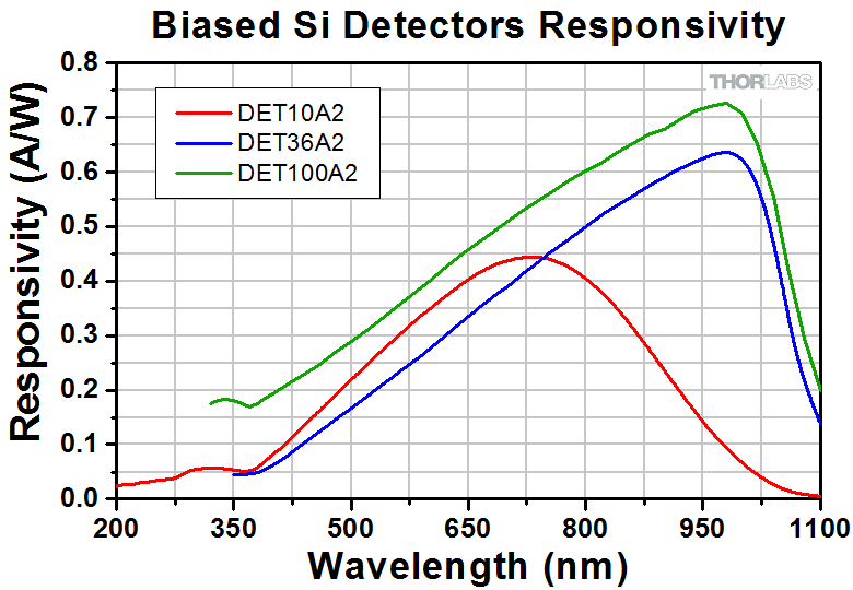 | |
| DET100A2 | 75.4 mm2 (Ø9.8 mm) | 320 - 1100 nm | 35 nsj (Typ.) | 10 MHzk | 2.4 x 10⁻¹⁴ W/Hz1/2 | 0.9 nA (Typ.) 10 nA (Max) | 150 pF (Typ.) | 10 V | ||
| DET36A2 | 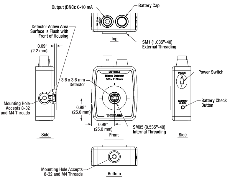 | 13 mm2 (3.6 x 3.6 mm)g | 350 - 1100 nm | 14 nsj (Typ.) | 25 MHzk | 1.6 x 10⁻¹⁴ W/Hz1/2 | 0.35 nA (Typ.) 6.0 nA (Max) | 40 pF (Typ.) | 10 V |
| Item #a | Housing Features | Active Area | Wavelength Rangeb | Rise / Fall Timeb,c,d | Bandwidthe | Noise-Equivalent Power (NEP) (Typ.)f | Dark Currentg | Junction Capacitance | Bias Voltage | Responsivity Plot (Raw Data) |
|---|---|---|---|---|---|---|---|---|---|---|
| DET20X2 | 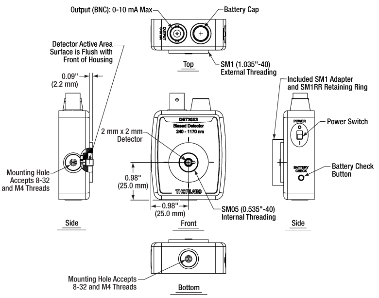 | 4 mm2 (2 x 2 mm)h | 240 - 1170 nm | 15 ns / 29 ns (Typ.) | 23.3 MHz | 7.1 x 10⁻¹⁵ W/Hz1/2 | 50 pA (Typ.) 1 nA (Max) | 13 pF (Typ.) | 10 V |  |
| Item #a | Housing Features | Active Area | Wavelength Range | Rise Timeb,c | Bandwidthd | Noise-Equivalent Power (NEP) (Typ.) | Dark Currente | Junction Capacitance | Bias Voltage | Responsivity Plot (Raw Data) |
|---|---|---|---|---|---|---|---|---|---|---|
| DET10N2 | 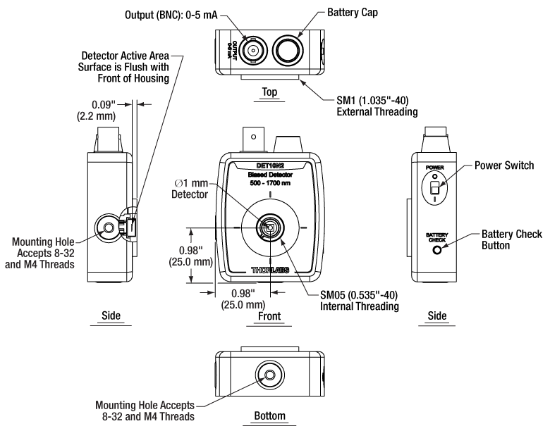 | 0.8 mm2 (Ø1.0 mm)f | 500 - 1700 nm | 5 nsg (Typ.) | 70 MHz | 2.0 x 10⁻¹⁴ W/Hz1/2 | 1.5 nA (Typ.) 10 nA (Max) | 50 pF (Typ.) | 5.0 V | 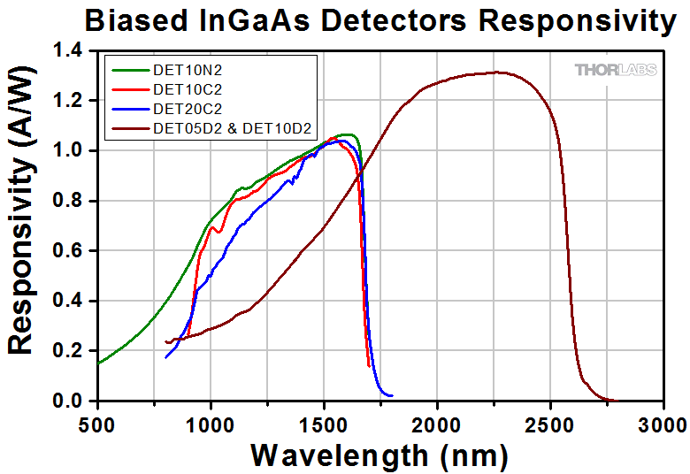 |
| DET20C2 |  | 3.14 mm2 (Ø2.0 mm)f | 800 - 1700 nm | 30 nsh (Typ.) | 11.7 MHz | 1.3 x 10⁻¹³ W/Hz1/2 | 55 nA (Typ.) 200 nA (Max) | 100 pF (Typ.) | 1.8 V | |
| DET10C2 | 0.8 mm2 (Ø1.0 mm)f | 900 - 1700 nm | 10 nsg (Typ.) | 35 MHz | 2.5 x 10⁻¹⁴ W/Hz1/2 | 1 nA (Typ.) 25 nA (Max) | 80 pF (Typ.) | 5.0 V | ||
| DET05D2 | 0.2 mm2 (Ø0.5 mm)f | 900 - 2600 nm | 17 nsh (Typ.) | 20.6 MHz | 1.0 x 10⁻¹² W/Hz1/2 | 2 µA (Typ.) 20 µA (Max) | 140 pF (Typ.) | 1.8 V | ||
| DET10D2 | 0.8 mm2 (Ø1.0 mm)f | 900 - 2600 nm | 25 nsh (Typ.) | 14 MHz | 1.5 x 10⁻¹² W/Hz1/2 | 5 µA (Typ.) 40 µA (Max) | 500 pF (Typ.) | 1.8 V |
| Item #a | Housing Features | Active Area | Wavelength Range | Rise Timeb,c | Bandwidthd | Noise-Equivalent Power (NEP) (Typ.) | Dark Currente | Junction Capacitance | Bias Voltage | Responsivity Plot (Raw Data) |
|---|---|---|---|---|---|---|---|---|---|---|
| DET50B2 | 19.6 mm2 (Ø5.0 mm)f | 800 - 1800 nm | 455 nsg (Typ.) | 770 kHz | 4.0 x 10⁻¹² W/Hz1/2 | 40 µA (Typ.) 80 µA (Max) | 4000 pF (Max) | 5.0 V | 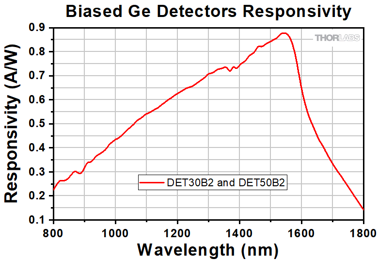 | |
| DET30B2 | 7.1 mm2 (Ø3.0 mm)f | 800 - 1800 nm | 650 nsh (Typ.) | 540 kHz | 2.6 x 10⁻¹² W/Hz1/2 | 4.0 µA (Max) | 6 nF (Max) | 1.8 V |
")
 ズーム
ズームA23は当社が現在販売しているDETフォトディテクタの交換用アルカリ電池です。バッテリ寿命が問題となる用途向けには、ACアダプタもご用意しています。詳細は下記をご参照ください。バッテリの期待寿命につきましては、上の「電池寿命」タブをご参照ください。

 ズーム
ズーム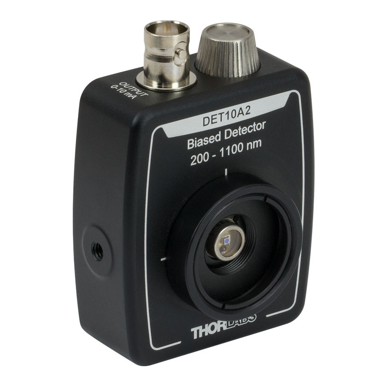
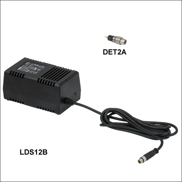
- DET2A: DETシリーズディテクタ用の電源アダプタ
- LDS12B: ±12 VDCの電源
- DET2B: DET2AとLDS12Bのセット
電源アダプタDET2A
DET2Aは、当社のDETシリーズディテクタ用の電源アダプタです。バッテリA23とバネ式のバッテリーキャップに代えて、電源LDS12B(別売り)をディテクタに接続して直接駆動することができます。また、カスタム接続用に電源ケーブルPDA-C-72と使用することもできます。DET2AとPDA-C-72を接続してDETシリーズディテクタに電源を供給する場合は、茶色(+12 V)および黒色(GND)のピンのみ使用します。
ACアダプタ LDS12B
LDS12Bは±12 VDCの安定化電源で、短絡やオーバーロードに対する保護用の電流リミット機能、LED表示付きのOn/Offスイッチ、AC入力電圧の切り替えスイッチ(100/120/230 VAC)が付いています。尚、電源LDS12Bには日本国内向けの電源ケーブルが付いています。
電源アダプターセットDET2B
電源アダプターセットDET2Bには電源アダプタDET2AとACアダプタLDS12Bが含まれています。こちらの電源アダプターセットは当社のDETシリーズのディテクタのバッテリの代わりにご使用可能です。ディテクタのバッテリとバネ式のバッテリーキャップを付属のアダプタDET2Aと交換し、電源LDS12Bの3ピンのプラグをアダプタに接続するだけでお使いいただけます。使用方法は、右の動画でご覧になれます。
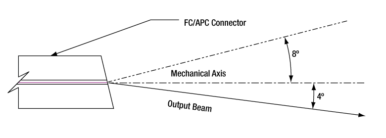
- FC/PC(ナローキーまたはワイドキー)、FC/APC(ナローキーまたはワイドキー)、SMA、ST®*/PC、SC/PC、 LC/PC、またはØ2.5 mmフェルールレセプタクル付き
- SM1レンズチューブとの組み合わせで遮光可能
- 当社の多くのフォトダイオードパワーセンサに対応
注: APCアダプタの前面には 2つの窪みがあり、スパナレンチSPW909またはSPW801を用いて締め付け可能です。このアダプタをSM1レンズチューブと遮光用途でお使いいただけるように、窪みはディスクを貫通していません。
FC/PCおよびFC/APCアダプタには、ナローキー(2.0 mm)とワイドキー(2.2 mm)の2種類のコネクタをご用意しております。ナローキーとワイドキーの詳細については、光ファイバとは のページをご覧ください。
フェルール用アダプタS120-25は、ロッキングコネクタ機構無しの設計になっています。Ø2.5 mmフェルール付きのファイバーパッチケーブルに対応し、フォトディテクタやパワーセンサを用いた測定を迅速に行うことができます。
| Item # | S120-FC2a | S120-FCa | S120-APC2b | S120-APCb | S120-SMA | S120-ST | S120-SC | S120-LC | S120-25a |
|---|---|---|---|---|---|---|---|---|---|
| Adapter Image (Click the Image to Enlarge) |  |  | 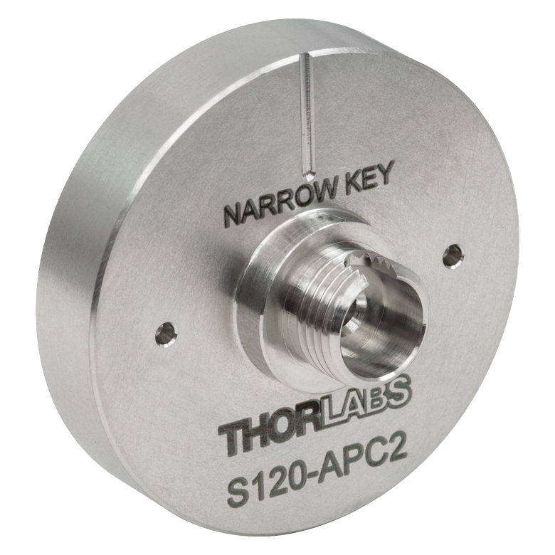 | 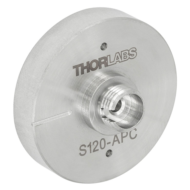 | 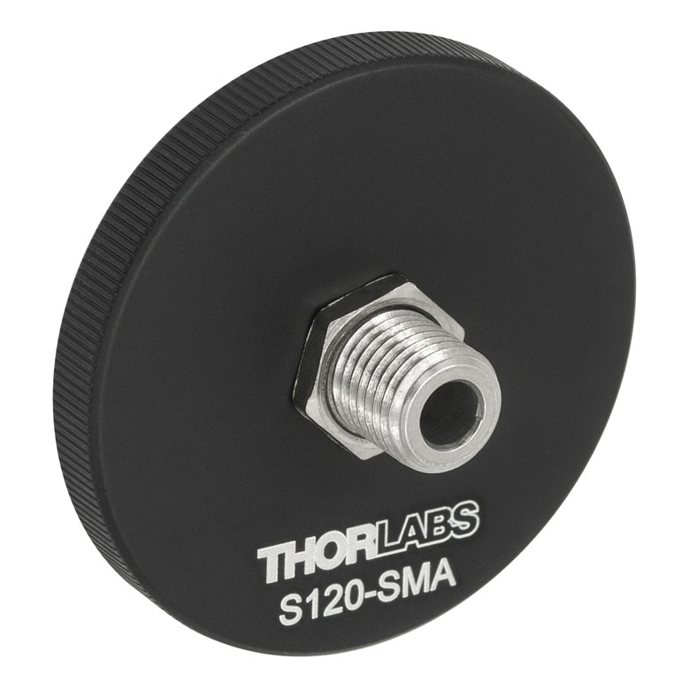 | 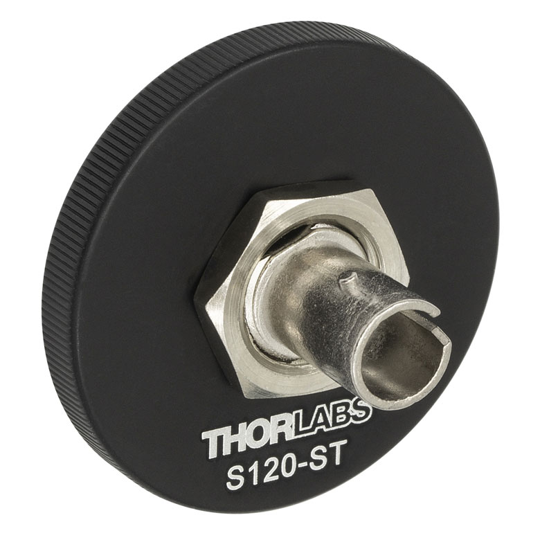 | 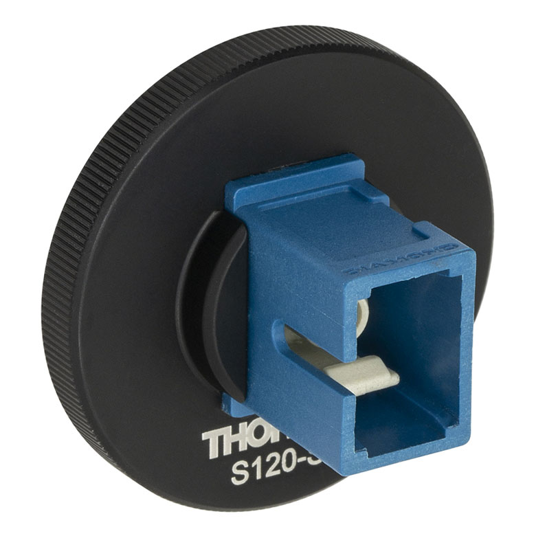 | 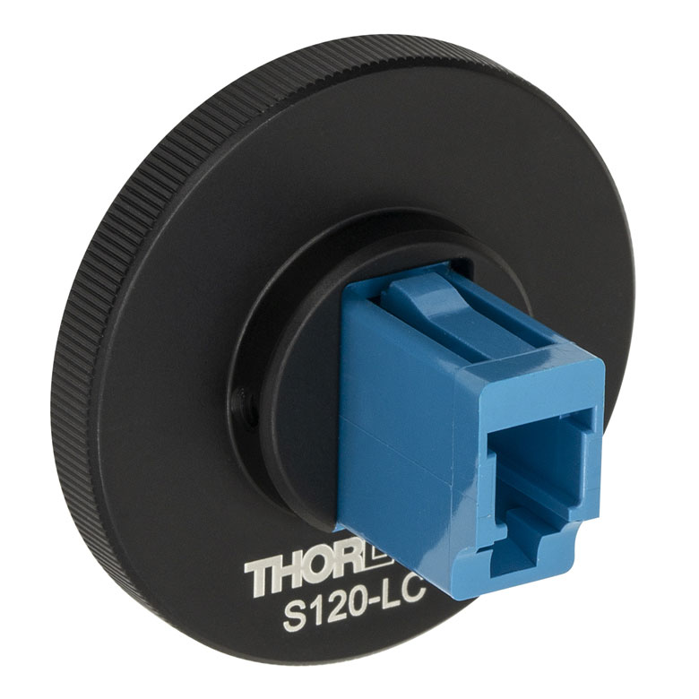 |  |
| Fiber Connector Type | FC/PC, 2.0 mm Narrow Key | FC/PC, 2.2 mm Wide Key | FC/APC, 2.0 mm Narrow Key | FC/APC 2.2 mm Wide Key | SMA | ST/PC | SC/PCc | LC/PC | Ø2.5 mm Ferrule |
| Threading | Internal SM1 (1.035"-40) | ||||||||
*ST®はLucent Technologies社の登録商標です。
- FC/PC(ナローキーまたはワイドキー)、FC/APC(ナローキーまたはワイドキー)、SMA、ST®*/PC、SC/PC、 LC/PCレセプタクル付き
- FC/PC(ワイドキー)とSMAレセプタクルは真空対応の製品もご用意
- SM1レンズチューブとの組み合わせで遮光可能
- 当社の多くの30 mmケージプレートならびにフォトディテクタに対応
注: 各ディスクには4つの窪み(前面と背面に2つずつ)があり、どちらの面からもスパナレンチSPW909またはSPW801で締め付け可能です。アダプタをSM1レンズチューブと遮光用途で使用できるよう、窪みはディスクを貫通していません。アダプタの位置確定後は、固定リングSM1RRで固定してください。
FC/PCおよびFC/APCアダプタには、ナローキー(2.0 mm)とワイドキー(2.2 mm)の2種類のコネクタをご用意しております。ナローキーとワイドキーの詳細については、光ファイバとはのページをご覧ください。
| Item # | SM1FC2 | SM1FC | SM1FCV | SM1FCA2a | SM1FCAa | SM1SMA | SM1SMAV | SM1ST | SM1SC1b | SM1LCb |
|---|---|---|---|---|---|---|---|---|---|---|
| Adapter Image (Click the Image to Enlarge) | 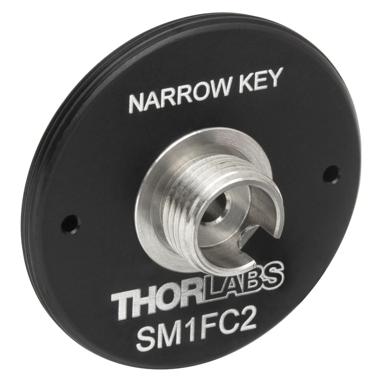 | 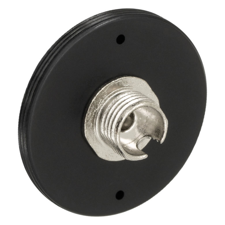 | 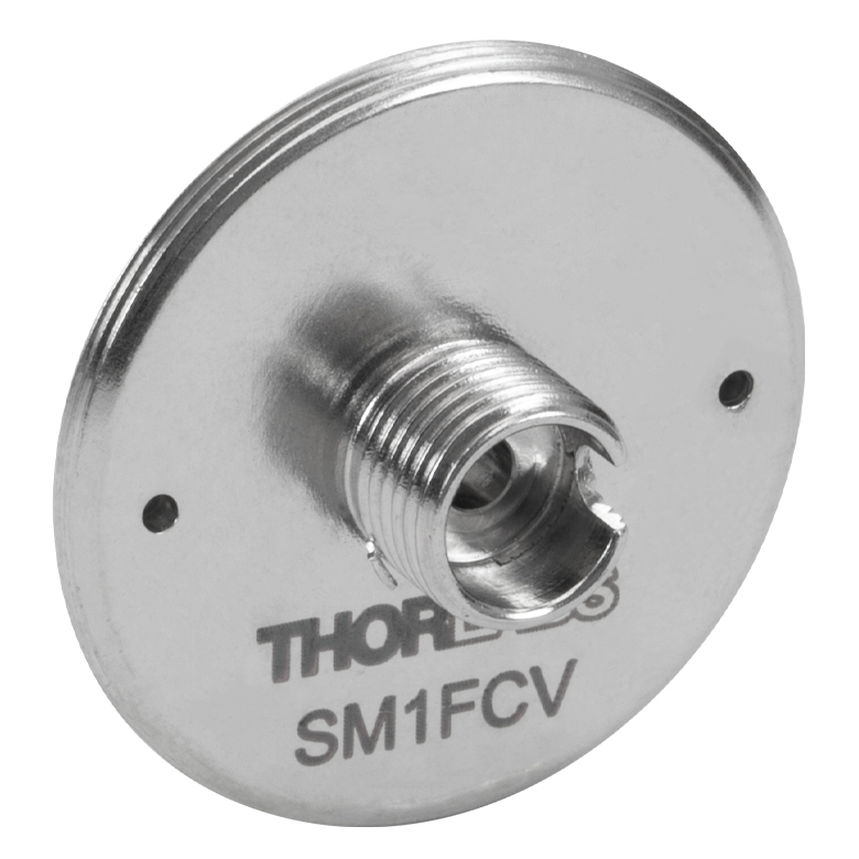 |  |  | 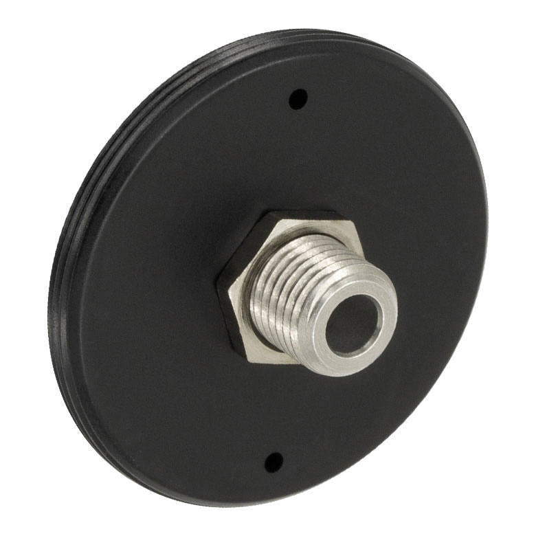 | 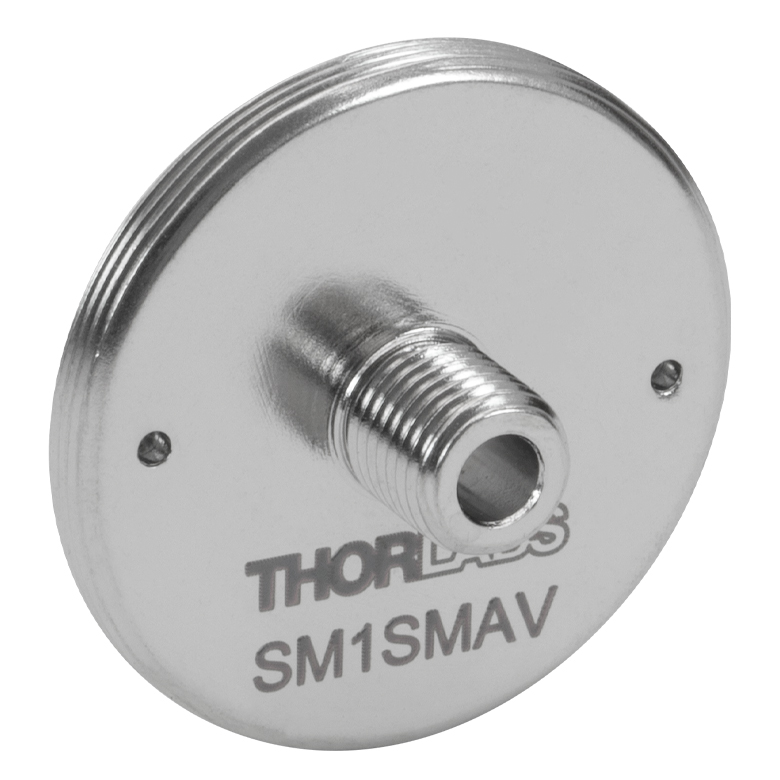 | 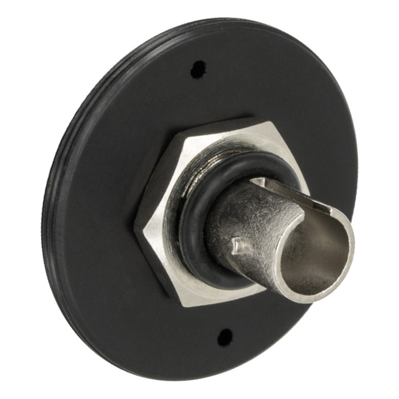 | 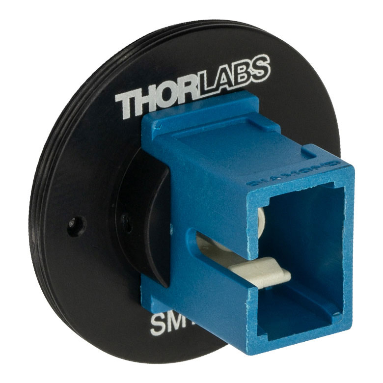 | 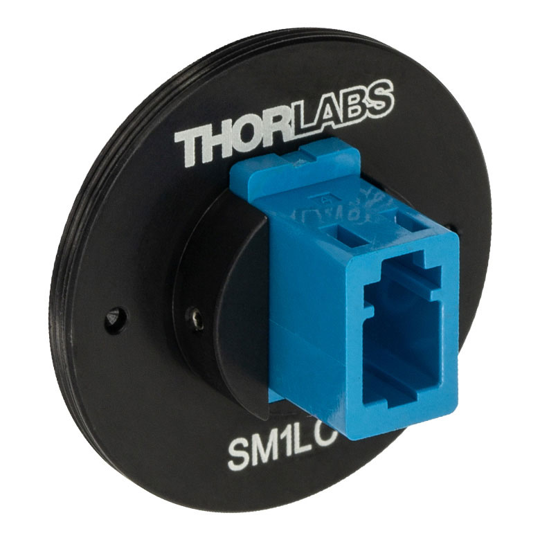 |
| Connector Type | FC/PC, 2.0 mm Narrow Key | FC/PC, 2.2 mm Wide Key | FC/PC, 2.2 mm Wide Key | FC/APC, 2.0 mm Narrow Key | FC/APC, 2.2 mm Wide Key | SMA | SMA | ST/PC | SC/PCc | LC/PC |
| Vacuum Compatibility | - | >10-10 Torr | - | >10-10 Torr | - | |||||
| Threading | External SM1 (1.035"-40) | |||||||||
*ST®はLucent Technologies社の登録商標です。