 Products Home
ビームサンプラー
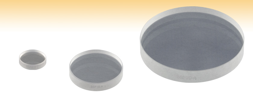
- Available in 1/2", 1", or 2" Diameter
- Fresnel Reflections at 45° for 1% to 10% Reflectance,
Depending on Polarization - AR-Coated Back Surface to Minimize Ghosting
- 0.5° Wedge to Eliminate Interference Fringes
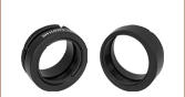
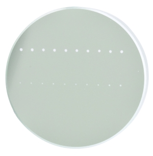
BSF05-A
Ø1/2"
BSF10-A
Ø1"
BSF20-A
Ø2"


Please Wait
| Specifications | |||
|---|---|---|---|
| Diameter | Ø1/2" (Ø12.7 mm) | Ø1" (Ø25.4 mm) | Ø2" (Ø50.8 mm) |
| Diameter Tolerance | +0.0/-0.2 mm | ||
| Thickness | 3 mm | 5 mm | 8 mm |
| Center Thickness Tolerance | ±0.1 mm | ±0.4 mm | |
| Material | UV Fused Silicaa | ||
| Surface Flatness | λ/10 @ 633 nm Over the Clear Aperture | ||
| Wedge | 30 ± 10 arcmin | ||
| Surface Quality | 20-10 (Scratch-Dig) | ||
| Front Surface Coating | None | ||
| Back Surface Coating | Broadband AR Coating R< 1.0% Average within Wavelength Range | ||
| Clear Aperture | > 90% of the Diameter | ||

| Damage Threshold Specifications | |
|---|---|
| Coating Designation (Item # Suffix) | Damage Threshold |
| -UV | 5.0 J/cm2 (355 nm, 10 ns, 10 Hz, Ø0.350 mm) |
| -A | 7.5 J/cm2 (532 nm, 10 ns, 10 Hz, Ø0.491 mm) |
| -B | 0.246 J/cm2 (800 nm, 99 fs, 1 kHz, Ø0.166 mm) 7.5 J/cm2 (810 nm, 10 ns, 10 Hz, Ø0.133 mm) |
| -C | 7.5 J/cm2 (1542 nm, 10 ns, 10 Hz, Ø0.189 mm) |
特長
- UV溶融石英(UVFS)基板
- サイズ:Ø12.7 mm(Ø1/2インチ)、Ø25.4 mm(Ø1インチ)、Ø50.8 mm(Ø2インチ)
- 裏面のARコーティングによりゴーストを最小化
- 干渉縞を除去する0.5°ウェッジ角
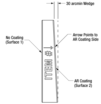
このビームサンプラでは、コーティングが施されていない光学素子の表面(「図」タブにあるように光学素子側面に表示)からのフレネル反射を使って、入射ビームの1~10%を分離します(入射光の偏光によります)。入射角45°とP偏光で、ビームスプリッタは約1%の反射率を示します。一方、S偏光は約10%の反射率を 示します。偏光および入射角を横軸にとったときの反射率プロットの詳細については「グラフ」タブを参照ください。
これらのレーザ品質ビームスプリッタは、透過ビームの損失および波面歪みを最小限に抑える必要があるモニタリング用途で一般的に使われています。裏面は内部の干渉縞を排除するためにウェッジ角が付けられていて、またゴーストを最小に抑えるためにARコーティングも施されています。ビームサンプラは、コーティングされていない前面から入射したビームを反射させ、背面からビームを透過させることにより、ビームコンバイナとして使用することも可能です。
ビームサンプラはUV溶融石英製です。この製品は広い使用温度範囲にわたり波面収差を最小に抑える必要のある用途に適しています。さらに、UV溶融石英はレーザによって引き起こされる蛍光(193 nmで測定)はほとんど見られず、UV域から近赤外域まで、様々な用途に適しています。
また、当社ではN-BK7製およびUV溶融石英製のウェッジウィンドウもご提供しています。どちらもコート無し、ARコーティング付きをお選びいただけます。
Click for Details
入射光量の数%をコーティング無し表面で反射させることによってビームをサンプリングします。
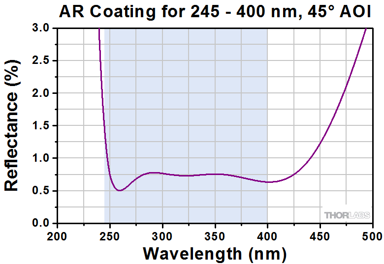
UV溶融石英(UVFS)ビームサンプラは、250~420 nm(-UV)、350~700 nm(-A)、650~1050 nm(-B)、1050~1700 nm(-C)の広帯域ARコーティング付きでご用意しております。この多層ARコーティングは、45°の入射角(NA0.5)用に設計されています。下のグラフは、当シリーズ製品の標準的なコーティングの波長特性を示しています。広帯域ARコーティングの典型的な吸収率は0.25%ですが、この反射率のグラフには反映されていません。
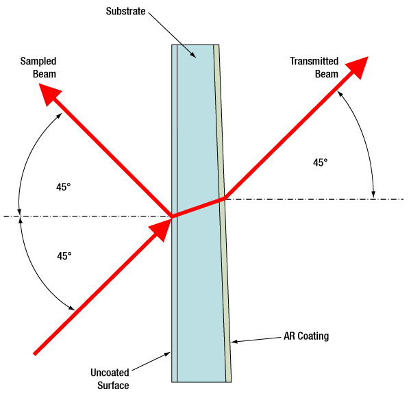
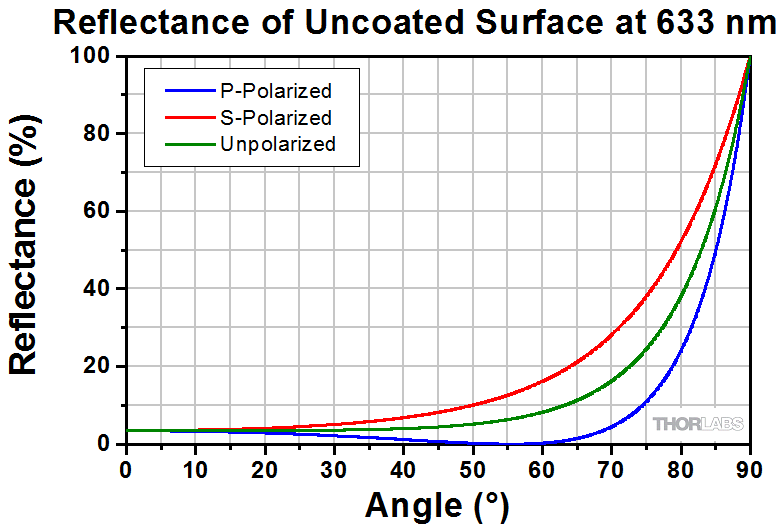
こちらのビームサンプラは、右図のようにビームをコーティング無し表面に入射させて使用します。下の左側のグラフは各コーティング範囲内、入射角0~90°での、よく使用される波長におけるコーティング無し表面の反射特性を示しています。
ビームサンプラ、ARコーティング:250~420 nm

Click to Enlarge
詳細データはこちらからダウンロードいただけます
サンプルビームは、ビームサンプラのコーティング無し表面から反射されたビームです。上のグラフでは、入射角の範囲内で光学素子のコーティング無し表面で反射したビームの光量を%で示しています。ミラーは入射角45°で最適化されています。
Click to Enlarge
詳細データはこちらからダウンロードいただけます
型番末尾が-UVのビームサンプラの背面は250~420 nmのARコーティング付きで、この面で透過光の後方反射を最小限に抑えます。
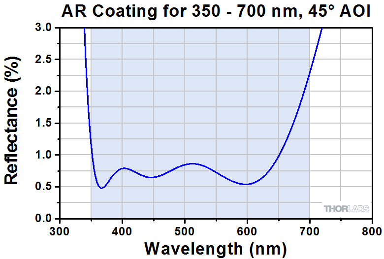
ビームサンプラ、ARコーティング:350~700 nm
Click to Enlarge
詳細データはこちらからダウンロードいただけます
サンプルビームは、ビームサンプラのコーティング無し表面から反射されたビームです。上のグラフでは、入射角の範囲内で光学素子のコーティング無し表面で反射したビームの光量を%で示しています。ミラーは入射角45°で最適化されています。
Click to Enlarge
詳細データはこちらからダウンロードいただけます
型番末尾が-Aのビームサンプラの背面は350~700 nmのARコーティング付きで、この面で透過光の後方反射を最小限に抑えます。
ビームサンプラ、ARコーティング:650~1050 nm
Click to Enlarge
詳細データはこちらからダウンロードいただけます
サンプルビームは、ビームサンプラのコーティング無し表面から反射されたビームです。上のグラフでは、入射角の範囲内で光学素子のコーティング無し表面で反射したビームの光量を%で示しています。ミラーは入射角45°で最適化されています。

Click to Enlarge
詳細データはこちらからダウンロードいただけます
型番末尾が-Bのビームサンプラの背面は650~1050 nmのARコーティング付きで、この面で透過光の後方反射を最小限に抑えます。
ビームサンプラ、ARコーティング:1050~1700 nm
Click to Enlarge
詳細データはこちらからダウンロードいただけます。
サンプルビームは、ビームサンプラのコーティング無し表面から反射されたビームです。上のグラフでは、入射角の範囲内で光学素子のコーティング無し表面で反射したビームの光量を%で示しています。ミラーは入射角45°で最適化されています。

Click to Enlarge
詳細データはこちらからダウンロードいただけます。
型番末尾が-Cのビームサンプラの背面は1050~1700 nmのARコーティング付きで、この面で透過光の後方反射を最小限に抑えます。
| Damage Threshold Specifications | |
|---|---|
| Coating Designation (Item # Suffix) | Damage Threshold |
| -UV | 5.0 J/cm2 (355 nm, 10 ns, 10 Hz, Ø0.350 mm) |
| -A | 7.5 J/cm2 (532 nm, 10 ns, 10 Hz, Ø0.491 mm) |
| -B | 0.246 J/cm2 (800 nm, 99 fs, 1 kHz, Ø0.166 mm) 7.5 J/cm2 (810 nm, 10 ns, 10 Hz, Ø0.133 mm) |
| -C | 7.5 J/cm2 (1542 nm, 10 ns, 10 Hz, Ø0.189 mm) |
当社のUV溶融石英製ビームサンプラの損傷閾値データ
右の仕様は当社のUV溶融石英製ビームサンプラの測定値です。損傷閾値の仕様はコーティングの種類が同じであればビームサンプラのサイズにかかわらず同じです。
レーザによる損傷閾値について
このチュートリアルでは、レーザ損傷閾値がどのように測定され、使用する用途に適切な光学素子の決定にその値をどのようにご利用いただけるかを総括しています。お客様のアプリケーションにおいて、光学素子を選択する際、光学素子のレーザによる損傷閾値(Laser Induced Damage Threshold :LIDT)を知ることが重要です。光学素子のLIDTはお客様が使用するレーザの種類に大きく依存します。連続(CW)レーザは、通常、吸収(コーティングまたは基板における)によって発生する熱によって損傷を引き起こします。一方、パルスレーザは熱的損傷が起こる前に、光学素子の格子構造から電子が引き剥がされることによって損傷を受けます。ここで示すガイドラインは、室温で新品の光学素子を前提としています(つまり、スクラッチ&ディグ仕様内、表面の汚染がないなど)。光学素子の表面に塵などの粒子が付くと、低い閾値で損傷を受ける可能性があります。そのため、光学素子の表面をきれいで埃のない状態に保つことをお勧めします。光学素子のクリーニングについては「光学素子クリーニングチュートリアル」をご参照ください。
テスト方法
当社のLIDTテストは、ISO/DIS 11254およびISO 21254に準拠しています。
初めに、低パワー/エネルギのビームを光学素子に入射します。その光学素子の10ヶ所に1回ずつ、設定した時間(CW)またはパルス数(決められたprf)、レーザを照射します。レーザを照射した後、倍率約100倍の顕微鏡を用いた検査で確認し、すべての確認できる損傷を調べます。特定のパワー/エネルギで損傷のあった場所の数を記録します。次に、そのパワー/エネルギを増やすか減らすかして、光学素子にさらに10ヶ所レーザを照射します。このプロセスを損傷が観測されるまで繰返します。損傷閾値は、光学素子が損傷に耐える、損傷が起こらない最大のパワー/エネルギになります。1つのミラーBB1-E02の試験結果は以下のようなヒストグラムになります。
上の写真はアルミニウムをコーティングしたミラーでLIDTテストを終えたものです。このテストは、損傷を受ける前のレーザのエネルギは0.43 J/cm2 (1064 nm、10 ns pulse、 10 Hz、Ø1.000 mm)でした。
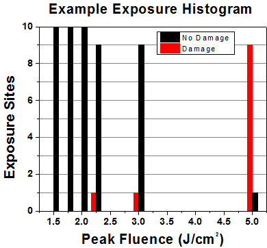
| Example Test Data | |||
|---|---|---|---|
| Fluence | # of Tested Locations | Locations with Damage | Locations Without Damage |
| 1.50 J/cm2 | 10 | 0 | 10 |
| 1.75 J/cm2 | 10 | 0 | 10 |
| 2.00 J/cm2 | 10 | 0 | 10 |
| 2.25 J/cm2 | 10 | 1 | 9 |
| 3.00 J/cm2 | 10 | 1 | 9 |
| 5.00 J/cm2 | 10 | 9 | 1 |
試験結果によれば、ミラーの損傷閾値は 2.00 J/cm2 (532 nm、10 ns pulse、10 Hz、 Ø0.803 mm)でした。尚、汚れや汚染によって光学素子の損傷閾値は大幅に低減されるため、こちらの試験はクリーンな光学素子で行っています。また、特定のロットのコーティングに対してのみ試験を行った結果ではありますが、当社の損傷閾値の仕様は様々な因子を考慮して、実測した値よりも低めに設定されており、全てのコーティングロットに対して適用されています。
CWレーザと長パルスレーザ
光学素子がCWレーザによって損傷を受けるのは、通常バルク材料がレーザのエネルギを吸収することによって引き起こされる溶解、あるいはAR(反射防止)コーティングのダメージによるものです[1]。1 µsを超える長いパルスレーザについてLIDTを論じる時は、CWレーザと同様に扱うことができます。
パルス長が1 nsと1 µs の間のときは、損傷は吸収、もしくは絶縁破壊のどちらかで発生していると考えることができます(CWとパルスのLIDT両方を調べなければなりません)。吸収は光学素子の固有特性によるものか、表面の不均一性によるものかのどちらかによって起こります。従って、LIDTは製造元の仕様以上の表面の質を有する光学素子にのみ有効です。多くの光学素子は、ハイパワーCWレーザで扱うことができる一方、アクロマティック複レンズのような接合レンズやNDフィルタのような高吸収光学素子は低いCWレーザ損傷閾値になる傾向にあります。このような低い損傷閾値は接着剤や金属コーティングにおける吸収や散乱によるものです。
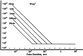
線形パワー密度におけるLIDTに対するパルス長とスポットサイズ。長パルス~CWでは線形パワー密度はスポットサイズにかかわらず一定です。 このグラフの出典は[1]です。

繰返し周波数(prf)の高いパルスレーザは、光学素子に熱的損傷も引き起こします。この場合は吸収や熱拡散率のような因子が深く関係しており、残念ながらprfの高いレーザが熱的影響によって光学素子に損傷を引き起こす場合の信頼性のあるLIDTを求める方法は確立されておりません。prfの大きいビームでは、平均出力およびピークパワーの両方を等しいCW出力と比較する必要があります。また、非常に透過率の高い材料では、prfが上昇してもLIDTの減少は皆無かそれに近くなります。
ある光学素子の固有のCWレーザの損傷閾値を使う場合には、以下のことを知る必要があります。
- レーザの波長
- ビーム径(1/e2)
- ビームのおおよその強度プロファイル(ガウシアン型など)
- レーザのパワー密度(トータルパワーをビームの強度が1/e2の範囲の面積で割ったもの)
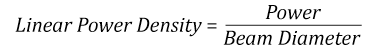
ビームのパワー密度はW/cmの単位で計算します。この条件下では、出力密度はスポットサイズとは無関係になります。つまり、スポットサイズの変化に合わせてLIDTを計算し直す必要がありません(右グラフ参照)。平均線形パワー密度は、下の計算式で算出できます。
ここでは、ビーム強度プロファイルは一定であると仮定しています。次に、ビームがホットスポット、または他の不均一な強度プロファイルの場合を考慮して、おおよその最大パワー密度を計算する必要があります。ご参考までに、ガウシアンビームのときはビームの強度が1/e2の2倍のパワー密度を有します(右下図参照)。
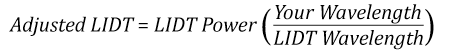
次に、光学素子のLIDTの仕様の最大パワー密度を比較しましょう。損傷閾値の測定波長が光学素子に使用する波長と異なっている場合には、その損傷閾値は適宜補正が必要です。おおよその目安として参考にできるのは、損傷閾値は波長に対して比例関係であるということです。短い波長で使う場合、損傷閾値は低下します(つまり、1310 nmで10 W/cmのLIDTならば、655 nmでは5 W/cmと見積もります)。
この目安は一般的な傾向ですが、LIDTと波長の関係を定量的に示すものではありません。例えば、CW用途では、損傷はコーティングや基板の吸収によってより大きく変化し、必ずしも一般的な傾向通りとはなりません。上記の傾向はLIDT値の目安として参考にしていただけますが、LIDTの仕様波長と異なる場合には当社までお問い合わせください。パワー密度が光学素子の補正済みLIDTよりも小さい場合、この光学素子は目的の用途にご使用いただけます。
当社のウェブ上の損傷閾値の仕様と我々が行った実際の実験の値の間にはある程度の差があります。これはロット間の違いによって発生する誤差を許容するためです。ご要求に応じて、当社は個別の情報やテスト結果の証明書を発行することもできます。損傷解析は、類似した光学素子を用いて行います(お客様の光学素子には損傷は与えません)。試験の費用や所要時間などの詳細は、当社までお問い合わせください。
パルスレーザ
先に述べたように、通常、パルスレーザはCWレーザとは異なるタイプの損傷を光学素子に引き起こします。パルスレーザは損傷を与えるほど光学素子を加熱しませんが、光学素子から電子をひきはがします。残念ながら、お客様のレーザに対して光学素子のLIDTの仕様を照らし合わせることは非常に困難です。パルスレーザのパルス幅に起因する光学素子の損傷には、複数の形態があります。以下の表中のハイライトされた列は当社の仕様のLIDT値が当てはまるパルス幅に対する概要です。
パルス幅が10-9 sより短いパルスについては、当社の仕様のLIDT値と比較することは困難です。この超短パルスでは、多光子アバランシェ電離などのさまざまなメカニクスが損傷機構の主流になります[2]。対照的に、パルス幅が10-7 sと10-4 sの間のパルスは絶縁破壊、または熱的影響により光学素子の損傷を引き起こすと考えられます。これは、光学素子がお客様の用途に適しているかどうかを決定するために、レーザービームに対してCWとパルス両方による損傷閾値を参照しなくてはならないということです。
| Pulse Duration | t < 10-9 s | 10-9 < t < 10-7 s | 10-7 < t < 10-4 s | t > 10-4 s |
|---|---|---|---|---|
| Damage Mechanism | Avalanche Ionization | Dielectric Breakdown | Dielectric Breakdown or Thermal | Thermal |
| Relevant Damage Specification | No Comparison (See Above) | Pulsed | Pulsed and CW | CW |
お客様のパルスレーザに対してLIDTを比較する際は、以下のことを確認いただくことが重要です。
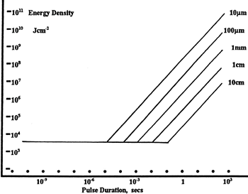
エネルギ密度におけるLIDTに対するパルス長&スポットサイズ。短パルスでは、エネルギ密度はスポットサイズにかかわらず一定です。このグラフの出典は[1]です。
- レーザの波長
- ビームのエネルギ密度(トータルエネルギをビームの強度が1/e2の範囲の面積で割ったもの)
- レーザのパルス幅
- パルスの繰返周波数(prf)
- 実際に使用するビーム径(1/e2 )
- ビームのおおよその強度プロファイル(ガウシアン型など)
ビームのエネルギ密度はJ/cm2の単位で計算します。右のグラフは、短パルス光源には、エネルギ密度が適した測定量であることを示しています。この条件下では、エネルギ密度はスポットサイズとは無関係になります。つまり、スポットサイズの変化に合わせてLIDTを計算し直す必要がありません。ここでは、ビーム強度プロファイルは一定であると仮定しています。ここで、ビームがホットスポット、または他の不均一な強度プロファイルの場合を考慮して、おおよその最大パワー密度を計算する必要があります。ご参考までに、ガウシアンビームのときは一般にビームの強度が1/e2のときの2倍のパワー密度を有します。
次に、光学素子のLIDTの仕様と最大エネルギ密度を比較しましょう。損傷閾値の測定波長が光学素子に使用する波長と異なっている場合には、その損傷閾値は適宜補正が必要です[3]。経験則から、損傷閾値は波長に対して以下のような平方根の関係であるということです。短い波長で使う場合、損傷閾値は低下します(例えば、1064 nmで 1 J/cm2のLIDTならば、532 nmでは0.7 J/cm2と計算されます)。
波長を補正したエネルギ密度を得ました。これを以下のステップで使用します。
ビーム径は損傷閾値を比較する時にも重要です。LIDTがJ/cm2の単位で表される場合、スポットサイズとは無関係になりますが、ビームサイズが大きい場合、LIDTの不一致を引き起こす原因でもある不具合が、より明らかになる傾向があります[4]。ここで示されているデータでは、LIDTの測定には<1 mmのビーム径が用いられています。ビーム径が5 mmよりも大きい場合、前述のようにビームのサイズが大きいほど不具合の影響が大きくなるため、LIDT (J/cm2)はビーム径とは無関係にはなりません。
次に、パルス幅について補正します。パルス幅が長くなるほど、より大きなエネルギに光学素子は耐えることができます。パルス幅が1~100 nsの場合の近似式は以下のようになります。
お客様のレーザのパルス幅をもとに、光学素子の補正されたLIDTを計算するのにこの計算式を使います。お客様の最大エネルギ密度が、この補正したエネルギ密度よりも小さい場合、その光学素子はお客様の用途でご使用いただけます。ご注意いただきたい点は、10-9 s と10-7 sの間のパルスにのみこの計算が使えることです。パルス幅が10-7 sと10-4 sの間の場合には、CWのLIDTも調べなければなりません。
当社のウェブ上の損傷閾値の仕様と我々が行った実際の実験の値の間にはある程度の差があります。これはロット間の違いによって発生する誤差を許容するためです。ご要求に応じて、当社では個別のテスト情報やテスト結果の証明書を発行することも可能です。詳細は、当社までお問い合わせください。
[1] R. M. Wood, Optics and Laser Tech. 29, 517 (1998).
[2] Roger M. Wood, Laser-Induced Damage of Optical Materials (Institute of Physics Publishing, Philadelphia, PA, 2003).
[3] C. W. Carr et al., Phys. Rev. Lett. 91, 127402 (2003).
[4] N. Bloembergen, Appl. Opt. 12, 661 (1973).

レーザーシステムが光学素子に損傷を引き起こすかどうか判断するプロセスを説明するために、レーザによって引き起こされる損傷閾値(LIDT)の計算例をいくつかご紹介します。同様の計算を実行したい場合には、右のボタンをクリックしてください。計算ができるスプレッドシートをダウンロードいただけます。ご使用の際には光学素子のLIDTの値と、レーザーシステムの関連パラメータを緑の枠内に入力してください。スプレッドシートでCWならびにパルスの線形パワー密度、ならびにパルスのエネルギ密度を計算できます。これらの値はスケーリング則に基づいて、光学素子のLIDTの調整スケール値を計算するのに用いられます。計算式はガウシアンビームのプロファイルを想定しているため、ほかのビーム形状(均一ビームなど)には補正係数を導入する必要があります。 LIDTのスケーリング則は経験則に基づいていますので、確度は保証されません。なお、光学素子やコーティングに吸収があると、スペクトル領域によってLIDTが著しく低くなる場合があります。LIDTはパルス幅が1ナノ秒(ns)未満の超短パルスには有効ではありません。
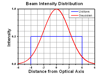
Figure 71A ガウシアンビームの最大強度は均一ビームの約2倍です。
CWレーザの例
波長1319 nm、ビーム径(1/e2)10 mm、パワー0.5 Wのガウシアンビームを生成するCWレーザーシステム想定します。このビームの平均線形パワー密度は、全パワーをビーム径で単純に割ると0.5 W/cmとなります。
しかし、ガウシアンビームの最大パワー密度は均一ビームの約2倍です(Figure 71A参照)。従って、システムのより正確な最大線形パワー密度は1 W/cmとなります。
アクロマティック複レンズAC127-030-CのCW LIDTは、1550 nmでテストされて350 W/cmとされています。CWの損傷閾値は通常レーザ光源の波長に直接スケーリングするため、LIDTの調整値は以下のように求められます。
LIDTの調整値は350 W/cm x (1319 nm / 1550 nm) = 298 W/cmと得られ、計算したレーザーシステムのパワー密度よりも大幅に高いため、この複レンズをこの用途に使用しても安全です。
ナノ秒パルスレーザの例:パルス幅が異なる場合のスケーリング
出力が繰返し周波数10 Hz、波長355 nm、エネルギ1 J、パルス幅2 ns、ビーム径(1/e2)1.9 cmのガウシアンビームであるNd:YAGパルスレーザーシステムを想定します。各パルスの平均エネルギ密度は、パルスエネルギをビームの断面積で割って求めます。
上で説明したように、ガウシアンビームの最大エネルギ密度は平均エネルギ密度の約2倍です。よって、このビームの最大エネルギ密度は約0.7 J/cm2です。
このビームのエネルギ密度を、広帯域誘電体ミラーBB1-E01のLIDT 1 J/cm2、そしてNd:YAGレーザーラインミラーNB1-K08のLIDT 3.5 J/cm2と比較します。LIDTの値は両方とも、波長355 nm、パルス幅10 ns、繰返し周波数10 Hzのレーザで計測しました。従って、より短いパルス幅に対する調整を行う必要があります。 1つ前のタブで説明したようにナノ秒パルスシステムのLIDTは、パルス幅の平方根にスケーリングします:
この調整係数により広帯域誘電体ミラーBB1-E01のLIDTは0.45 J/cm2に、Nd:YAGレーザーラインミラーのLIDTは1.6 J/cm2になり、これらをビームの最大エネルギ密度0.7 J/cm2と比較します。広帯域ミラーはレーザによって損傷を受ける可能性があり、より特化されたレーザーラインミラーがこのシステムには適していることが分かります。
ナノ秒パルスレーザの例:波長が異なる場合のスケーリング
波長1064 nm、繰返し周波数2.5 Hz、パルスエネルギ100 mJ、パルス幅10 ns、ビーム径(1/e2)16 mmのレーザ光を、NDフィルタで減衰させるようなパルスレーザーシステムを想定します。これらの数値からガウシアン出力における最大エネルギ密度は0.1 J/cm2になります。Ø25 mm、OD 1.0の反射型NDフィルタ NDUV10Aの損傷閾値は355 nm、10 nsのパルスにおいて0.05 J/cm2で、同様の吸収型フィルタ NE10Aの損傷閾値は532 nm、10 nsのパルスにおいて10 J/cm2です。1つ前のタブで説明したように光学素子のLIDTは、ナノ秒パルス領域では波長の平方根にスケーリングします。
スケーリングによりLIDTの調整値は反射型フィルタでは0.08 J/cm2、吸収型フィルタでは14 J/cm2となります。このケースでは吸収型フィルタが光学損傷を防ぐには適した選択肢となります。
マイクロ秒パルスレーザの例
パルス幅1 µs、パルスエネルギ150 µJ、繰返し周波数50 kHzで、結果的にデューティーサイクルが5%になるレーザーシステムについて考えてみます。このシステムはCWとパルスレーザの間の領域にあり、どちらのメカニズムでも光学素子に損傷を招く可能性があります。レーザーシステムの安全な動作のためにはCWとパルス両方のLIDTをレーザーシステムの特性と比較する必要があります。
この比較的長いパルス幅のレーザが、波長980 nm、ビーム径(1/e2)12.7 mmのガウシアンビームであった場合、線形パワー密度は5.9 W/cm、1パルスのエネルギ密度は1.2 x 10-4 J/cm2となります。これをポリマーゼロオーダ1/4波長板WPQ10E-980のLIDTと比較してみます。CW放射に対するLIDTは810 nmで5 W/cm、10 nsパルスのLIDTは810 nmで5 J/cm2です。前述同様、光学素子のCW LIDTはレーザ波長と線形にスケーリングするので、CWの調整値は980 nmで6 W/cmとなります。一方でパルスのLIDTはレーザ波長の平方根とパルス幅の平方根にスケーリングしますので、1 µsパルスの980 nmでの調整値は55 J/cm2です。光学素子のパルスのLIDTはパルスレーザのエネルギ密度よりはるかに大きいので、個々のパルスが波長板を損傷することはありません。しかしレーザの平均線形パワー密度が大きいため、高出力CWビームのように光学素子に熱的損傷を引き起こす可能性があります。
| Posted Comments: | |
cdolbashian
(posted 2024-06-24 04:19:04.0) Thank you for reaching out to us with this custom request. We can potentially change these components as you describe above. I have put you in contact with our customs team in order to fulfil this request. For future custom requests, feel free to email Techsales@thorlabs.com. Callum Watt
(posted 2024-06-12 15:37:07.667) Hi, I have read in a previous comment bellow that a marker indicating the position of the thicker end of the wedge was suggested to your internal engineering forum (comment on 2018-04-12). Has there been any update on this request? Is the orientation of the wedge with respect to the uncoated surface marker always the same? jpolaris
(posted 2024-06-21 01:35:01.0) Thank you for contacting Thorlabs. The engineering effort required to mark the wedge's thickest point on every beam sampler manufactured is not feasible for us at this time. However, I have reached out to you directly to discuss the possibility of fulfilling this request as a special order. Malo Raoul
(posted 2024-05-16 14:08:28.62) Hello, we are using the BSF10-C as a beam combiner, combining the light on the S1 face and we would like to know if you offer a product without the wedge, and only coated on one side. Thank you cdolbashian
(posted 2024-05-28 10:59:45.0) Thank you for reaching out to us with this inquiry. What you want seems to be a non-wedged, UVFS window which is only AR coated on one side. We can definitely do this as a custom. I have reached out to you directly in order to facilitate a custom such as this. prathmesh ghag
(posted 2023-10-18 12:43:45.79) I have a circularly polarized collimated beam. I want to sample the light out by intensity division. But I dont want to change the original circularity. Can you suggest a solution for this application?
Also do you have non polarizing samplers giving approx 1-5% of the intensity? Fabio Novelli
(posted 2023-02-28 16:42:23.523) Hello,
What is the typical Transmission % for a p-polarized beam at 45 degrees?
Is R+T>99% for BSF10-B?
Best,
Fabio jgreschler
(posted 2023-03-02 02:26:34.0) Thank you for reaching out to Thorlabs. You can see a graph and download the raw data of the reflectance in the "graphs" tab of this product page. At 45 degrees, the P polarized reflectance percentage is 0.7433. user
(posted 2022-04-23 17:00:27.21) Hi team, a perhaps very naïve question: what is the difference between your beam sampler and non-polarising beam splitter products? Is it just that the latter has a wider range of specified split ratio, while the former relies on just the Fresnel reflection? Are there certain use cases I should pick one over the other? Thanks in advance. jdelia
(posted 2022-05-12 01:25:50.0) Thank you for contacting Thorlabs. A beam sampler utilizes Fresnel reflections of an uncoated optical surface to pick off about 1-10% of the light, which is also dependent on the polarization of the light. Beam splitters have a dielectric coating optimized for a chosen wavelength range deposited on the front surface. The beam samplers also have a 0.5 degree wedge to eliminate interference fringes. Additionally, like you mentioned, the beamsplitters have a larger range of R:T ratios, while the beam sampler is generally intended for 1-10%, though this can change with angle. I have contacted you directly to discuss your application. Lin Su
(posted 2021-06-28 01:11:25.323) Is the reflectivity curve different for S and P polarization for the AR coated surface? Do you have data on it? Thanks in advance! YLohia
(posted 2021-06-28 02:33:36.0) Hello Lin, the data presented here is the average of the S and P polarization reflectivities. I have reached out to you directly with curves for S and P reflectivities (theoretical). Garnet Cameron
(posted 2020-09-14 17:03:43.247) The reflectance graph provided is for 45 degree AOI. Is this AR coating the same for WW41050-C? I am interested in the R at 8 degree AOI. YLohia
(posted 2020-09-15 01:16:16.0) We have at least two versions of the UV/VIS/NIR/telecom AR coatings (-UV, -A, -B, -C) -- one designed for 0 degrees AOI (on windows, lenses, etc), and one designed at 45 degrees (on the beam samplers). I have reached out to you directly with data. Steffen Hädrich
(posted 2020-07-27 11:16:22.94) What is the AR coating characteristic at close to AOI=0° (likely 5-10°). Can you please send curves or data on this? nbayconich
(posted 2020-07-27 03:33:05.0) Thank you for contacting Thorlabs. Please see the link below to our AR coating curves below, we have reflection plots for the –UV, -A, -B & -C coatings measured at 8° AOI.
https://www.thorlabs.com/newgrouppage9.cfm?objectgroup_id=5840&tabname=AR%20coating user
(posted 2019-07-24 23:30:41.78) Dear supportor
I’m Jongkeun Yang in south korea.
I have a interesting about BSF10-A.
So, would you please inform me that reflectance (%) of 400 to 700 nm wavelength?
Thanks tcampbell
(posted 2019-07-25 09:51:54.0) Hello, thank you for contacting Thorlabs. Reflectance data for these beam samplers can be found on the Graphs tab. Sai Kanth Dacha
(posted 2019-03-19 17:36:34.507) I purchased a BSF10-C recently. I have a 1064 nm laser that is putting out linearly polarized, ~138 uJ, 1.3 ns pulses at 1 kHz. The input beam, about 3.1 mm wide, is incident on the uncoated surface. I am observing significant ghosting in reflection: I can see, on the IR card, two distinct spots with similar brightness. Isn't the AR coating supposed to prevent this? I'm pretty sure that I'm well below the damage threshold as well. Please let me know if this has been reported before. nbayconich
(posted 2019-04-01 11:00:39.0) Thank you for contacting Thorlabs. The reflection off the AR coated surface should be less than 1.0%. Depending on the sensitivity of your viewing card if the incident source has enough power the ghost reflection could still be detectable.
What angle of incidence is your source on the un-coated surface of the beam sampler? Is your source S or P polarized with respect to the beam sampler's un-coated surface?
It would be best to know the exact power measurements of your reflected beams. A techsuppport representative will reach out to you directly to discuss your application. caleb.anderson
(posted 2018-07-05 14:39:38.37) Hello,
I've got a high power laser diode stack (Max power ~600 W) of which I am trying to characterize the wavelength. However, the spectrometers I have come across have either extremely low LIDTs or would be saturated by the laser beam. I don't currently have a way to characterize the width of the beam as it is complex, and it is in the IR spectrum, so it cannot be visibly characterized. Would I be able to use this to sample a portion of the beam in a spectrometer, at least at lower power levels? YLohia
(posted 2018-07-06 08:43:40.0) You can use the beam sampler you were looking at to reduce the amount of power going into your spectrometer and avoid saturation. Alternately, you could use one of the neutral density filters from this page as well for a more specific attenuation: https://www.thorlabs.com/navigation.cfm?guide_id=2185 user
(posted 2018-04-11 07:46:40.983) Any change to add the marking for the wedge's widest point? YLohia
(posted 2018-04-12 09:35:55.0) Hello, thank you for contacting Thorlabs. Marking the wedge's widest point was one of the ideas suggested to be able to tell the back and front surfaces apart from each other. As a solution to this problem, we have implemented an engraved arrow that points towards the uncoated surface. That being said, I have posted your request for a marking for the widest point in our internal engineering forum. user
(posted 2015-10-01 21:20:38.99) Good product, but these windows have serious birefringence. We were using these before a half wave plate/ polarizing beamsplitter and were troubleshooting why the extinction ratio was so poor; it was because our sampler was making the beam semi-circularly polarized. You should mention this somewhere in the datasheet. besembeson
(posted 2015-10-09 11:42:58.0) Response from Bweh at Thorlabs USA: Thanks for the feedback. According to our tests though, we have not seen any birefringence from these. Birefringence can be introduced if the optic is clamped too hard. Maybe you try less-tightening when holding the optic. arlen.biersgreen.1
(posted 2015-08-07 13:35:42.59) How do I calculate the offset in the transmitted beam from my incident beam? That is, what are the relevant coefficients of refraction for the layers on the sampler so that I can do the calculation? Thanks. jlow
(posted 2015-08-25 03:39:55.0) Response from Jeremy at Thorlabs: You can see the UVFS refractive index graph at http://www.thorlabs.com/newgrouppage9.cfm?objectgroup_id=6973&tabname=UV%20Fused%20Silica. The AR coating is very thin relative to the substrate so the offset from that should be negligible. However, the back surface does have a 0.5° angle relative to the front surface so that would needs to be taken into account. chris.middleton
(posted 2015-04-24 13:04:12.707) I believe the beam samplers would work better with your standard mirror mounts (e.g., KM100) if the AR coating was on the non-wedged surface. Assuming that (1) you want to be incident (45 deg) on the the uncoated surface and (2) that you want the cylindrical surface of the BSF to be concentric with the mount's well that accepts the optic, you can get twice as much beam clearance if the AR coating was on the non-wedged surface. Contact me if you would like drawings. cdaly
(posted 2015-04-29 08:28:10.0) Response from Chris at Thorlabs: Thank you for your feedback. The uncoated surface is the one from which the beam would be sampled. In the KM100 mount this would put this face towards the front face of the mount, seated against the internal lip. These beam samplers can also be used with the clear edge mount for 1" optics (KM1CE) or clear quadrant mounts for 1/2" optics. (KM05FL/KM05FR) if any further beam clearance is required. jhinr
(posted 2014-02-28 12:07:15.517) Hello,
I am interested in the spectral response (transmission and refelction) for a broad wavelength range. We are looking for a beam sampler for monitoring in a spectroscopic application, where we look at signals from 400nm to about 2.2um, and we could only use one beam sampler (there is not much space available). Hence it would be nice to know how the transmission and reflection are affected by the coatings in this range. Do you have any data about this?
Regards,
Johannes Hinrichs besembeson
(posted 2014-03-05 02:31:41.0) Response from Bweh E. at Thorlabs: We have the theoretical reflectivity graphs for these AR coatings outside the design wavelength range. I will share these with you via email. xxu
(posted 2014-02-20 21:51:04.297) The propagation direction of the transmitted beam is changed after the beam sampler. Because there is no marking of which direction the wedge between the front and back surface of the sampler is, I cannot rotate the beam sampler to at least make the beam stay in the vertical or horizontal plane.
I think this beam sampler is of little help for systems that needs high precision alignment. cdaly
(posted 2014-02-25 05:14:04.0) Response from Chris at Thorlabs: Thank you for your feedback. I agree some sort of marking, at the wedge's widest point for example, would make it easier to keep the beam in given plane. We will discuss this internally. Perhaps we can have one added in the future. iraj.kavosh
(posted 2013-12-10 11:11:30.427) Hi, Please include:
(1) Laser damage threshold for CW & Pulsed modes
(2) Reflectivity vs wavelength in case the laser wavelength is outside of the Sampler range. Or, we need to split off more power by selecting a different Sampler.
Thanks. jlow
(posted 2014-01-08 04:53:50.0) Response from Jeremy at Thorlabs: The pulsed damage threshold located in the overview tab on the webpage, under the specifications table. For the BSF10-C, it is 7.5 J/cm^2 (1542 nm, 10 ns, 10 Hz, Ø0.189 mm). For CW, we do not have a laser with high enough power to destroy the coating. The BSF10-C was able to withstand around 3 kW/cm without being damaged. We can provide out of band reflectivity. I will get in contact with you directly to provide this. johanna.tragardh
(posted 2013-08-12 16:24:54.82) Hi, I would like to use the beam sampler to pick off light from a broad band (tuneable) laser. What is the reflectivity of the AR coating substantially outside the range (say 350-2000 nm for the visible coating?) Your graph ends at 2%. Alternatively is it possible to get these beam samplers without AR coating? jlow
(posted 2013-08-12 10:37:00.0) Response from Jeremy at Thorlabs: The reflectivity of the AR coating is going to be quite high outside of the specified region. For the uncoated version, we have the stock WW41050 (http://www.thorlabs.com/newgrouppage9.cfm?objectgroup_id=5546&pn=WW41050) available which have better surface quality and flatness. wwbsghr
(posted 2013-01-28 09:45:47.287) Dear Sir/Madam, I would like to know the damage threshold for BSF10-UV.Can it be used as sampler for 10Hz laser(283nm,50mj/pulse,D3mm;355nm,180mj/pulse,D5mm)? bdada
(posted 2012-03-15 11:21:00.0) Response from Buki at Thorlabs to zhgaom:
Thank you for participating in our feedback forum. The damage threshold for our UVFS beam samplers is 5J/cm^2 for an 810nm laser, 10ns, 10Hz, with spot size of 0.158mm. Based on the data you provided, our beam samplers should be suitable. Please test one and contact TechSupport@thorlabs.com if you experience any issues. zhgaom
(posted 2012-03-14 02:08:11.0) Dear Sir/Madam,
I would like to know the damage threshold for BSF5-UV and BSF5-A. We currently have two lasers. One is Nd:YAG working at 220mJ@532nm and 20mJ @266nm. The typical repetition rate is 5Hz. As the beam diameter is 5mm, it gives the power/energy density as and 5.5W/cm^2, 1.1J/cm^2, respectively. The other laser we have is a Nd:YLF laser working at 527nm, typical pulse energy is 25mJ@1000Hz. Would you have proper beam sampler so that I can sample those laser and monitor them using a energy meter? Greg
(posted 2010-11-16 10:22:46.0) A response from Greg at Thorlabs: We recently performed damage threshold testing for a number of our optics. Among the tested optics was a B coated UVFS beam sampler. At this time, this is the only beam sampler that has undergone damage threshold testing. As we continue damage threshold testing, we will add more values to our website. The 100 mJ/cm2 mentioned in a previous feedback was a very conservative estimate before we performed damage threshold testing. If you would like more information regarding a product, please contact techsupport@thorlabs.com and we will be able to assist you further. user
(posted 2010-11-16 10:00:45.0) Is the damage threshold of the B coating (650-1050 nm) really higher than the others?
Actually, 100mJ/cm2 is mentioned in this post, whereas "5 J/cm2 (810 nm, 10 ns, 10 Hz)" is written for the B serie. Adam
(posted 2010-05-04 13:02:59.0) A response from Adam at Thorlabs to Sunqingzhen: All of the beam samplers should contain an arrow that points towards the uncoated surface. Since the arrow is drawn on, it is possible that the arrow was rubbed away. In the future we will use our engraver to ensure this does not happen. If you would like to test which surface is the coated surface, we suggest one of the following approaches:
Use a magnifier and look from the edge of the substrate in and you can see where the coating begins. Or you can hold in your hand on a angle and reflect the ambient light and see the coated side.
If you have trouble locating this surface we can exchange the unit for you. Adam
(posted 2010-05-04 12:59:20.0) A response from Adam at Thorlabs to sunqingzhen: The beam samplers do have an AR coating on the back surface that is meant to minimize the ghosting effect. Please note that this will not eliminate the ghosting effect especially for high power sources. I would like to contact you directly to get more information about your application. sunqingzhen
(posted 2010-05-03 23:20:07.0) I still have seen the ghosting, when the polarized laser is incident on the beam sampler at an angle of 45 degrees. sunqingzhen
(posted 2010-05-03 23:05:26.0) There is only a letter F on the sige of the beam sampler. Which is the AR coated surface?
I hadnt seen any arrow on the beam sampler! apalmentieri
(posted 2009-10-20 16:12:59.0) A response from Adam at Thorlabs: There should also be an arrow on the side of this optic. This arrow will point to the Ar coated surface. pmd
(posted 2009-10-20 15:54:32.0) The only mark on the edge of the optic is a letter F. With this mark how can I tell which is the AR coated surface? apalmentieri
(posted 2009-09-16 17:58:46.0) A response from Adam at Thorlabs: Currently we do not have beam splitters that can handle more power than 100mJ/cm^2. I will email you to try and get more information on the exact power of your Nd:Yag so I can find out if we can suggest any items that may work. daniel.fink
(posted 2009-09-16 17:45:52.0) Is there an alternative beam splitter which can handle more power than 100mJ/cm^2 as described below? What would you suggest for an 532nm ND:YAG laser? The splitted beam shall be used for power measurements and should have sth. like 5 to 10 % of the power. Thank you apalmentieri
(posted 2009-07-14 18:22:00.0) A response from Adam at Thorlabs: We are able to supply custom wavelength beamsplitters, but would require more information before we provide a quotation. I will contact you directly to get this information. hujianming
(posted 2009-07-14 16:58:14.0) Can you supply a beamsplitter with 400-900nm wavelength? If ok,how about the price?
Thank you very much. apalmentieri
(posted 2009-06-19 13:39:25.0) A response from Adam at Thorlabs: The damage threshold for these beamsamplers depend on the AR coatings. Currently, we can only provide an approximate damage threshold, which is 100W/cm^2 for CW laser and 100mJ/cm^2 for 10ns pulsed light. Please let me know if you have further questions. walter.schmoll
(posted 2009-06-19 09:45:56.0) How much power or pulse energy can these beam samplers handle? Greg
(posted 2009-03-23 15:19:33.0) A response from Greg at Thorlabs to dyanali: Thank you for your interest in our Beam Samplers. We have reflectivity data for these at 635 nm under the Graphs tab. We do not have data at 251 nm, but the reflection should be relatively consistent with the data at 635 nm. dyanali
(posted 2009-03-23 09:54:32.0) Hello,
What are the losses and reflectivity I can expect if I use one of the UVFS beam samplers to monitor a beam at 251nm?
Regards
Dyan Laurie
(posted 2008-03-31 16:05:32.0) Response from Laurie at Thorlabs to flickingerd: Thank you for noticing the typo under our specifications tab for the wedge angle. We have corrected that typo. As for the UV fused silica beam samplers, I have personally emailed you the theoretical reflectivity curve as a function of wavelength. Youll note that for 355 nm incident light, the average reflectivity for S and P polarized light incident at a 45 degree angle will be approximately 6%. Broadband coatings become more difficult to fabricate for shorter wavelengths; however, I have passed your suggestion for UV-coated beam samplers on to our optics engineers so that they can consider producing them in the future. Thank you for your interest in our products! flickingerd
(posted 2008-03-31 13:20:50.0) While Im at it, the wedge angle spec for the beam samplers (under the Specs tab) is written incorrectly, I think. Its written 30[deg] +/- 10 Arc Min, where [deg] is the little circle. The little circle should probably be replaced by a single quote, or the words "Arc Min" to avoid confusion. flickingerd
(posted 2008-03-31 13:11:53.0) About the UV fused silica beam samplers (BSF): why would you not offer your UV AR coating on your UV fused silica beam samplers? I would like one with the UV AR coating for use with a UV laser, but its probably not worth the wait to have one specially made right now. If you could email me the reflection off of the "A" coating for 355nm for now, that would be nice. technicalmarketing
(posted 2008-01-23 09:36:42.0) Dear Europe,
The laser windows are more expensive than the beam samplers because they have better scratch/dig specifications, they are coated on both sides, and the specialty coatings combined with the smaller production runs increase the cost per coating. europe
(posted 2008-01-22 10:16:40.0) Why are the Laser Windows (e.g. WG11050) more expensive than the beam samplers? Surface specs and product is nearly the same - and the sampler got even a wedge...? |