 Products Home
差分増幅フォトディテクタ、高速モニタ出力

- Models Available with Bandwidths Up to 2.5 GHz
- Noise Cancellation by Subtraction of 2 Input Signals
- >20 dB Common Mode Rejection Ratio
- Fast Monitor Outputs
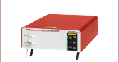
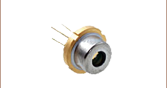
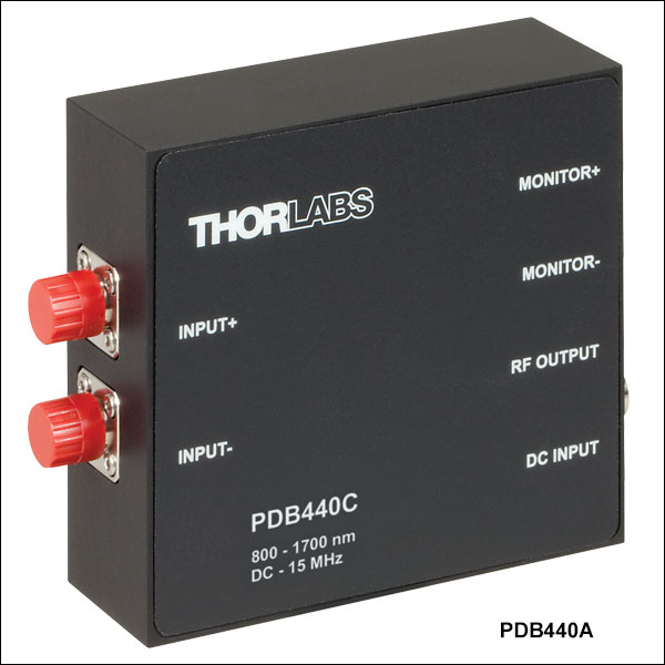
PDB415A
Fixed Gain, 100 MHz, Si
Optical Inputs Shown
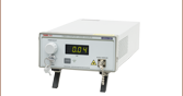
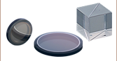
PDB450C
Switchable Gain, InGaAs
Optical Inputs Shown
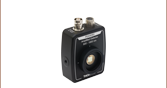
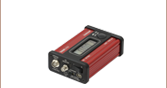
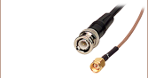
PDB482C-AC
Fixed Gain, 2.5 GHz, InGaAs, AC Coupled
Electrical Outputs Shown


Please Wait
| Balanced Detector Selection Guide |
|---|
| Balanced Detectors with Fast Monitor Output |
| Large-Area Balanced Amplified Detectors |
| Suitable for OCT |
| Compact Balanced Amplified Detectors |
| Compact Balanced Detectors |
| OCT Balanced Detectors with Fast Monitor Output |
| Auto-Balanced Detector with Avalanche Photodiodes |
一般的な用途
- 分光法
- ヘテロダイン検出
(「ドップラーLiDAR」タブ参照) - 光コヒーレンストモグラフィ(OCT)
- 光遅延測定
- THz検出
| Balanced Detector with Fast Monitor Output | |||
|---|---|---|---|
| Bandwidth | Available Wavelength Ranges | Fast Monitor Output Bandwidth | Gain |
| Switchable (DC - 0.1, 0.3, 4, 45, or 150 MHz) | 320 to 1000 nm or 800 - 1700 nm | DC - 1 MHz | Switchable |
| DC - 15 MHz | Fixed | ||
| DC - 75 MHz | |||
| DC - 100 MHz | |||
| DC - 200 MHz | |||
| DC - 350 MHz | |||
| DC - 400 MHz | Optimized for 1060 nm (900 - 1400 nm Range) or Optimized for 1300 nm (1200 - 1700 nm Range) | DC - 3 MHz | |
| DC - 500 MHz | 800 - 1700 nm | DC - 1 MHz | |
| 30 kHz - 1.0 GHz | Optimized for 1060 nm (900 - 1400 nm Range) | DC - 3 MHz | |
| 30 kHz - 1.6 GHz | Optimized for 1300 nm (1200 - 1700 nm Range) | DC - 3 MHz | |
| 1 MHz - 2.5 GHz | Optimized for 1060 nm (900 - 1400 nm Range) | DC - 2.5 MHz | |
特長
- 4つの波長範囲でご提供
- 320~1000 nm
- 800~1700 nm
- 900~1400 nm (1060 nmで最適化)
- 1200~1700 nm (1300 nmで最適化)
- コモンモードの除去比>20 dB
- 高速モニタ出力
- ディテクタはSiまたはInGaAsから選択可能
- 全ての製品でFCファイバ入力が可能
- 一部の製品は自由空間光入力が可能(詳細は下記参照)
- AC入力電圧切替え式のAC電源が付属
- トランスインピーダンス利得の切替え可能な製品もご用意
差分フォトディテクタは、2つの光入力信号の差分をとることにより、コモンモードノイズを除去します。それにより、信号経路上の微弱な信号の変化を干渉ノイズフロアの中から抽出することができます。
このディテクタは 2つの差分フォトダイオードと、超低ノイズの高速トランスインピーダンスアンプで構成されています。2つのフォトダイオードは優れたコモンモード除去比(CMRR)が得られるように整合されており、そのためノイズ除去性能がさらに向上しています。詳細は「動作」タブをご覧ください。全てのディテクタにはノイズ低減のために電気信号用の3つのメス型SMAポートが付いています。トランスインピーダンスアンプからのRF出力ポート以外にMonitor+とMonitor-のポートがありますが、これらを使用して各フォトダイオードの応答を個別にモニタすることができます。
入力信号の連続光成分(無変調成分)をブロックするため、どのモデルにもAC結合型をご用意しております。なお、PDB480C-AC、PDB481C-AC、PDB482C-ACはAC結合型のみをご用意しています。AC結合型を使用すると、増幅器を飽和する可能性のある強い連続光の背景信号があるときに、比較的弱い周波数変調信号の検出性能を改善することができます。AC結合型の低周波側カットオフ周波数は、PDB480C-AC、PDB481C-AC、PDB482C-AC、PDB835C-AC以外では100 Hz以下が保証されていますが、通常は5 Hzを下回ります。
帯域幅350 MHz以下のディテクタ
帯域幅がDC~350 MHz(またはそれ以下)のディテクタには、320~1000 nm用のSiフォトダイオード、または800~1700 nm用のInGaAsフォトダイオードを用いた製品がございます。これらのディテクタのフォトダイオードにはファイバは結合されていません。一方で取外し可能なFC入力コネクタが2つ付属しているため、自由空間光の入力にもファイバからの光入力にもご利用いただけます。ディテクタPDB465およびPDB435のセンサにもファイバは結合されていませんが、入力ポートに付いているFC/PCアダプタは取り外しができません。
これらのディテクタは 85 mm x 80 mm x 30 mmのアルミニウム製の筐体に収納されています。筐体の底面または側面に付属のアダプタープレートを付属のM2ネジで取付けると、ディテクタをポストに取付けることができます。
帯域幅400 MHz以上のディテクタ(PDB835シリーズを除く)
PDB835シリーズ以外の帯域幅がDC~400 MHz(またはそれ以上)のディテクタでは、ファイバ結合型フォトダイオードを使用しています。これらのディテクタのフォトダイオードは、全帯域幅に渡って優れたCMRR値が得られるように長さを正確に整合したファイバ(SMF-28e+またはHI1060 )で、FC/APC光入力ポートに接続されています。これらの全てのディテクタにはInGaAsフォトダイオードが組み込まれており、1060 nm(900~1400 nm)または1300 nm(1200~1700 nm)に最適化されています。またファイバ結合型であるため、ディテクタとの間に結合用光学素子を使用した場合に通常発生するOCT画像のラインアーチファクトが抑制されます。
最も広い帯域幅の差分ディテクタ(PDB480C-AC、PDB481C-AC、PDB482C-AC)では、AC結合型のみをご用意しています。最大帯域幅は2.5 GHzで、速度は大幅に向上しています。超低歪みの出力段はA/Dコンバーターカードへの入力電圧範囲として2 Vp-pまでサポートしているので、ファイバ結合型であることと併せてOCTの画像品質向上に大きく貢献しています。
これらのディテクタは 85 mm x 80 mm x 30 mmのアルミニウム製の筐体に収納されています。筐体の底面または側面に付属のアダプタープレートを付属のM2ネジで取付けると、ディテクタをポストに取付けることができます。
PDB835シリーズ超低ノイズディテクタ(DC~500 MHz、アーティファクト無し)
ディテクタPDB835CおよびPDB35C-ACでは、800~1700 nm用のInGaAsフォトダイオードがFC/APC入力ポートと自由空間を介して接続されています。内蔵のトランスインピーダンスアンプは、500 MHzまでの全動作帯域で超低ノイズを維持します(最小NEPの詳細については「仕様」タブをご覧ください)。これらのディテクタには、それぞれのフォトダイオードに個別にアライメントされたFC/APCコネクタが付いており、アーティファクト無しで動作します。各ディテクタの筐体は76.7 mm x 60.0 mm x 20.0 mmと小型で、上面と底面には#8-32とM4 x 0.7のどちらも使える取付けネジ穴があります。
電源
各ディテクタには±12 V DC出力の電源が付属します。交換用の電源も別途ご用意しております( 下記をご覧ください)。
当社では、差分ディテクタを内蔵したファイバベースの干渉計もご用意しています。主に光コヒーレンストモグラフィ(OCT)システムでの差分ディテクタの利用を検討されている場合は、こちらでOCT用途に適した製品をご覧いただけます。
| Item # | PDB415A(-AC) | PDB415C(-AC) | PDB425A(-AC) | PDB425C(-AC) | PDB435A(-AC) | PDB435C(-AC) |
|---|---|---|---|---|---|---|
| Detector Type | Si/PIN | InGaAs/PIN | Si/PIN | InGaAs/PIN | Si/PIN | InGaAs/PIN |
| Wavelength Range | 320 - 1000 nm | 800 - 1700 nm | 320 - 1000 nm | 800 - 1700 nm | 320 - 1000 nm | 800 - 1700 nm |
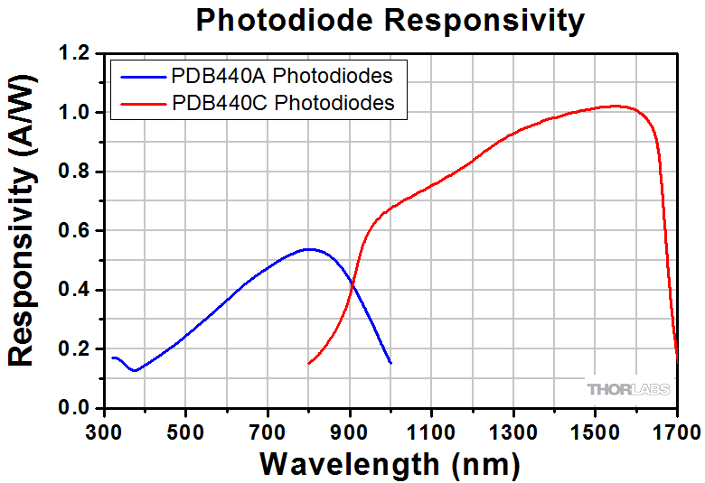
| Max Responsivity (Typical) | 0.53 A/W | 1.0 A/W | 0.53 A/W | 1.0 A/W | 0.50 A/W | 1.0 A/W |
| Active Detector Diameter | 0.8 mm | 0.3 mm | 0.8 mm | 0.3 mm | 0.4 mm | 0.15 mm |
| Bandwidth (3 dB) | DC - 100 MHz AC Coupled (-AC Suffix): 100 Hz - 100 MHz | DC - 75 MHz AC Coupled (-AC Suffix): 100 Hz - 75 MHz | DC - 350 MHz AC Coupled (-AC Suffix): 100 Hz - 350 MHz | |||
| Common Mode Rejection Ratio | > 25 dB | > 35 dB | > 20 dB | |||
| Transimpedance Gaina | 50 x 103 V/A | 250 x 103 V/A | 10 x 103 V/A | |||
| Minimum NEPb | 12.03 pW/Hz1/2 (DC - 100 MHz) | 6.99 pW/Hz1/2 (DC - 100 MHz) | 9.5 pW/Hz1/2 (DC - 75 MHz) | 5.2 pW/Hz1/2 (DC - 75 MHz) | 32.3 pW/Hz1/2 (DC - 350 MHz) | 15.28 pW/Hz1/2 (DC - 350 MHz) |
| RF Output | ||||||
| Conversion Gain RF Outputa,c | 26.5 x 10³ V/W | 50 x 103 V/W | 133 x 103 V/W | 250 x 103 V/W | 5 x 10³ V/W | 10 x 103 V/W |
| CW Saturation Power RF Output | 135 µW @ 820 nm | 72 µW @ 1550 nm | 27 µW @ 820 nm | 15 µW @ 1550 nm | 720 µW @ 820 nm | 360 µW @ 1550 nm |
| Impedance | 50 Ω | |||||
| Max Voltage Swing | ±1.8 V for 50 Ω Load ±3.6 V for High-Impedance Load | |||||
| DC Offset | < ±3 mV | |||||
| RF-Output Coupling | DC or AC | |||||
| Monitor Outputs | ||||||
| Conversion Gain Monitor Outputs | 10 V/mW @ 820 nm | 10 V/mW @ 1550 nm | 10 V/mW @ 820 nm | 10 V/mW @ 1550 nm | 10 V/mW @ 820 nm | 10 V/mW @ 1550 nm |
| Impedance | 220 Ω | |||||
| Max Voltage Swing | 1.55 V for 50 Ω Load 10 V for High-Z Load | |||||
| Bandwidth | DC to 1 MHz | |||||
| Voltage Noise | < 180 µVRMS | |||||
| DC Offset | < ±2 mV | |||||
| General | ||||||
| Fiber Optical Inputsd | FC/PC or FC/APC (Removable) | FC/PC or FC/APC (Not Removable) | ||||
| Photodiode Damage Threshold | 20 mW | |||||
| Electrical Outputs | SMA (Qty. 3) | |||||
| Dimensions | 85 mm x 80 mm x 30 mm (3.35" x 3.15" x 1.18") | |||||
| Weight | 0.35 kg (without Power Supply) | |||||
| Operating Temperature Rangee | 0 to 40 °C | |||||
| Storage Temperature Range | -40 to 70 °C | |||||
| Included Power Supplyf | ±12 V @ 250 mA (100/120/230 VAC, 50 - 60 Hz, Switchable) | |||||
| Item # | PDB440A(-AC) | PDB440C(-AC) | PDB450A(-AC) | PDB450C(-AC) | PDB465A(-AC) | PDB465C(-AC) |
|---|---|---|---|---|---|---|
| Detector Type | Si/PIN | InGaAs/PIN | Si/PIN | InGaAs/PIN | Si/PIN | InGaAs/PIN |
| Wavelength Range | 320 - 1000 nm | 800 - 1700 nm | 320 - 1000 nm | 800 - 1700 nm | 320 - 1000 nm | 800 - 1700 nm |
| Max Responsivity (Typical) | 0.53 A/W | 1.0 A/W | 0.53 A/W | 1.0 A/W | 0.50 A/W | 1.0 A/W |
| Active Detector Diameter | 0.8 mm | 0.3 mm | 0.8 mm | 0.3 mm | 0.8 mm | 0.15 mm |
| Bandwidth (3 dB) | DC - 15 MHz AC Coupled (-AC Suffix): 100 Hz - 15 MHz | DC - 150, 45, 4, 0.3, 0.1 MHz AC Coupled (-AC Suffix): 100 Hz - 150, 45, 4, 0.3, 0.1 MHz | DC - 200 MHz AC Coupled (-AC Suffix): 100 Hz - 200 MHz | |||
| Common Mode Rejection Ratio | > 35 dB | > 25 dB | > 25 dB | |||
| Transimpedance Gaina | 51 x 103 V/A | 103, 104, 105, 106, 107 V/A | 30 x 103 V/A | |||
| Minimum NEPb | 6.9 pW/Hz1/2 (DC - 15 MHz) | 3.9 pW/Hz1/2 (DC - 15 MHz) | DC - 0.1 MHz: 1.4 pW/Hz1/2 DC - 0.3 MHz: 1.1 pW/Hz1/2 DC - 4.0 MHz: 3.3 pW/Hz1/2 DC - 45 MHz: 28.9 pW/Hz1/2 DC - 150 MHz: 123 pW/Hz1/2 | DC - 0.1 MHz: 0.7 pW/Hz1/2 DC - 0.3 MHz: 0.5 pW/Hz1/2 DC - 4.0 MHz: 1.55 pW/Hz1/2 DC - 45 MHz: 14.9 pW/Hz1/2 DC - 150 MHz: 68.6 pW/Hz1/2 | 22.86 pW/Hz1/2 (DC - 200 MHz) | 8.52 pW/Hz1/2 (DC - 200 MHz) |
| RF Output | ||||||
| Conversion Gain RF Outputa,c | 27 x 103 V/W | 51 x 103 V/W | 0.53 x 10³ V/W, 0.53 x 10⁴ V/W, 0.53 x 10⁵ V/W, 0.53 x 10⁶ V/W, 0.53 x 10⁷ V/W | 103 V/W, 104 V/W, 105 V/W, 106 V/W, 107 V/W | 16 x 103 V/W | 30 x 103 V/W |
| CW Saturation Power RF Output | 130 µW @ 820 nm | 70 µW @ 1550 nm | 9 mW @ 820 nm | 4.5 mW @ 1550 nm | 225 µW @ 820 nm | 120 µW @ 1550 nm |
| Impedance | 50 Ω | |||||
| Max Voltage Swing | ±1.8 for 50 Ω Load ±3.6 V for High-Impedance Load | ±4.6 V (103 to 106 Gain)a ±10 V (107 Gain)a | ±1.8 for 50 Ω Load ±3.6 V for High-Impedance Load | |||
| DC Offset | < ±3 mV | < ±15 mV | < ±3 mV | |||
| RF-Output Coupling | DC or AC | |||||
| Monitor Outputs | ||||||
| Conversion Gain Monitor Outputs | 10 V/mW @ 820 nm | 10 V/mW @ 1550 nm | 10 V/mW @ 820 nm | 10 V/mW @ 1550 nm | 10 V/mW @ 820 nm | 10 V/mW @ 1550 nm |
| Impedance | 220 Ω | |||||
| Max Voltage Swing | 1.55 V for 50 Ω Load 10 V for High-Z Load | |||||
| Bandwidth | DC to 1 MHz | |||||
| Voltage Noise | < 180 µVRMS | |||||
| DC Offset | < ±2 mV | |||||
| General | ||||||
| Fiber Optical Inputsd | FC/PC or FC/APC (Removable) | FC/PC or FC/APC (Not Removable) | ||||
| Photodiode Damage Threshold | 20 mW | |||||
| Electrical Outputs | SMA (Qty. 3) | |||||
| Dimensions | 85 mm x 80 mm x 30 mm (3.35" x 3.15" x 1.18") | |||||
| Weight | 0.35 kg (without Power Supply) | |||||
| Operating Temperature Rangee | 0 to 40 °C | |||||
| Storage Temperature Range | -40 to 70 °C | |||||
| Included Power Supplyf | ±12 V @ 250 mA (100/120/230 VAC, 50 - 60 Hz, Switchable) | |||||
| Item # | PDB470C(-AC) a | PDB471C(-AC) a | PDB480C-AC a | PDB481C-AC a | PDB482C-AC a | PDB835C(-AC) a |
|---|---|---|---|---|---|---|
| Detector | ||||||
| Detector Type | InGaAs/PIN | |||||
| Optical Inputs | FC/APC | |||||
| Internal Coupling Fiber | SMF-28e+ | HI1060 | SMF-28e+ | HI1060 | None | |
| Coupling Loss | < 0.5 dB (< 0.3 dB Typ.) | < 1.0 dB (< 0.4 dB Typ.) | < 0.5 dB (< 0.3 dB Typ.) | < 1.0 dB (<0.4 dB Typ.) | N/A | |
| Operating Wavelength | Optimized for 1300 nm (1200 - 1700 nm Range) | Optimized for 1060 nm (900 - 1400 nm Range) | Optimized for 1300 nm (1200 - 1700 nm Range) | Optimized for 1060 nm (900 - 1400 nm Range) | 800 - 1700 nm | |
| Responsivity (Typical) | 0.9 A/W @ 1550 nm | 0.72 A/W @ 1060 nm | 0.9 A/W @ 1550 nm | 0.72 A/W @ 1060 nm | 1.0 A/W @ 1550 nm | |
| Active Detector Diameter | 0.075 mm | 0.080 mm | 0.075 mm | 0.08 mm | ||
| Optical Back Reflection | < -40 dB | N/A | ||||
| Photodiode Damage Threshold | 10 mW | 5 mW | 10 mW | 5 mW | 20 mW | |
| RF OUTPUT | ||||||
| RF OUTPUT Bandwidth (3 dB) | DC - 400 MHz AC Coupled (-AC Suffix): 100 Hz - 400 MHz | 30 kHz - 1.6 GHz | 30 kHz - 1.0 GHz | 1 MHz - 2.5 GHz | DC - 500 MHz AC Coupled (-AC Suffix): 1 kHz - 500 MHz | |
| Common Mode Rejection Ratio | > 25 dB (Typ. >30 dB) | > 20 dB (Typ. > 25 dB) | > 25 dB | |||
| RF OUTPUT Transimpedance Gain | 10 x 10 3 V/A b | 16 x 10 3 V/A c | 28 x 10 3 V/A c | 10 x 10 3 V/A d | ||
| RF OUTPUT Conversion Gain | 9 x 10 3 V/W @ 1550 nm b | 7.2 x 10 3 V/W @ 1060 nm b | 14.4 x 10 3 V/W @ 1550 nm c | 11.5 x 10 3 V/W @ 1060 nm c | 20 x 10 3 V/W @ 1060 nm c | 10 x 10 3 V/W @ 1550 nm d,e |
| RF OUTPUT Power at 1 dB Compression c | - | +16.5 dBm Min +18 dBm Typ. | - | |||
| RF OUTPUT CW Saturation Power | 420 µW @ 1550 nm | 530 µW @ 1060 nm | See Note Below | 360 µW @ 1550 nm | ||
| RF OUTPUT Coupling | DC or AC | AC Coupling Only | DC or AC | |||
| RF OUTPUT Impedance | 50 Ω | |||||
| Max Voltage Swing | ±1.9 V for 50 Ω Load ±3.8 V for High-Z Load | See Note Below | ±1.8 V for 50 Ω Load; ±3.6 V (Linear Over 0 to 2.5 V) for High-Z Load | |||
| Minimum NEP f | 8 pW/Hz 1/2 (DC to 100 MHz) | 9.3 pW/Hz 1/2 (30 kHz to 100 MHz) | 9.0 pW/Hz 1/2 (30 kHz to 100 MHz) | 12.0 pW/Hz 1/2 (1 MHz to 100 MHz) | 6.5 pW/Hz 1/2 (DC to 500 MHz) | |
| Overall Output Voltage Noise | < 2.0 mV RMS | < 9 mV RMS | < 6.5 mV RMS | < 12 mV RMS | < 1.5 mV RMS | |
| DC Offset | N/A | < ±5 mV | ||||
| MONITOR Outputs | ||||||
| MONITOR Output Impedance | 200 Ω | |||||
| MONITOR Output Bandwidth (3 dB) | DC - 3 MHz | DC - 2.5 MHz | DC - 1 MHz | |||
| MONITOR Output Conversion Gain, High Z Load b | 9 V/mW @ 1550 nm | 7.2 V/mW @ 1060 nm | 9 V/mW @ 1550 nm | 7.2 V/mW @ 1060 nm | 10 V/mW @ 1550 nm e | |
| MONITOR Output Voltage Swing | 10 V Max, High Z Load | 1.5 V Max for 50 Ω Load 10 V Max (Linear Over 0 to 5 V) for High-Z Load | ||||
| Overall Output Voltage Noise | < 0.65 mV RMS | < 0.6 mV RMS | ||||
| DC Offset | < ±2 mV | < ±5 mV | ||||
| General | ||||||
| Electrical Outputs | SMA | |||||
| Included DC Power Supply g | ±12 V @ 250 mA (100/120/230 VAC, 50 - 60 Hz, Switchable) | |||||
| Operating Temperature Range h | 0 °C to 40 °C | |||||
| Storage Temperature Range | -40 °C to 70 °C | |||||
| Dimensions (W x H x D) | 85 mm x 80 mm x 30 mm (3.35" x 3.15" x 1.18") | 76.7 mm x 60.0 mm x 20.0 mm (3.02" x 2.36" x 0.79") | ||||
| Weight | 0.35 kg | 0.13 kg | ||||
注:
PDB480C-AC、PDB481C-AC、PDB482C-ACについてはRF出力信号が1 dB圧縮点におけるRF出力パワーを超過してはいけません。1 dB圧縮点とは、1 GHzの増幅信号において、線形増幅の理想直線から出力が1 dB落ちる点です。この値を超えると、増幅信号は非線形になり、飽和し始めます。この飽和点におけるRF出力電圧は次の式で算出できます:
![]()
ここで、Rは負荷インピーダンスで50Ω、P0は1 mWとし、L(dBm)はdBm表記の出力レベルです。仕様表に記載された1dB圧縮点におけるRF出力パワー16.5 dBmを用いると、次の"最大"出力電圧が算出されます:

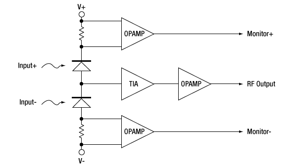
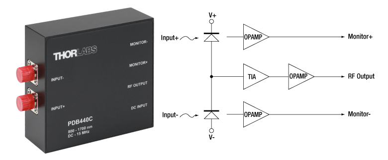
帯域幅500 MHz以下の差分ディテクタの動作
当社の差分増幅フォトディテクタは、2つの整合性のとれたフォトダイオードと超低雑音高速インピーダンスアンプ(TIA)で構成されています。TIAは2つのフォトダイオードの光電流(2つの光入力信号)の差分に比例した出力電圧(RF OUTPUT)を生成します。また、差分増幅フォトディテクタには、それぞれ個々のフォトダイオードの入力パワーレベルを確認するために、2つの高速モニタ出力ポート(MONITOR+と MONITOR-)が付いています。このポートの出力周波数は低いので、信号のRF変調の測定には使用できません。下記は、当社の帯域幅500 MHz以下の差分ディテクタのブロック図です。
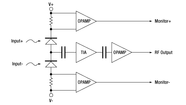
差分ディテクタPDB480C-AC、 PDB481C-AC、PDB482C-ACの動作
差分増幅フォトディテクタPDB48xC-ACは、上記の差分ディテクタと動作原理は同じですが、いくつかの機能が付加されています。こちらのディテクタのTIAの超低歪みの出力ステージは、2 Vp-pA/Dのコンバーターカードの入力電圧範囲をサポートします。また、2つの高速モニタ出力を使用して、個々の光入力パワーレベルの測定だけではなく、3 MHz(型番PDB480C-AC、PDB481C-AC)または2.5 MHz (型番PDB482C-AC)までの低周波の変調信号の測定にご使用いただけます。より高い周波数にも対応させるため、フォトダイオードは長さを揃えたファイバで入力ポートに接続されており、AC結合型のみをご用意しています。また、回路中のTIAの前後にコンデンサを追加しています(下図参照)。
差分増幅フォトディテクタのピン配列
モニタ +/-
SMA メス型
最大電圧:Hi-Z(ハイインピーダンス)に対しては+10 V、50 Ω負荷抵抗に対しては+1.5 Vです。
RF出力
SMA メス型
フォトディテクタPDB415、PDB425、PDB440、PDB465、PDB835のRF出力電圧の最高値は、Hi-Z(ハイインピーダンス)に対しては±3.6 V、50 Ω負荷抵抗に対しては±1.8 Vとなります。
PDB470CおよびPDB471CのRF出力のCW飽和出力は、それぞれ420 µW@1550 nm、530 µW@1060 nmです。
フォトディテクタPDB48xC-ACの50 Ω負荷抵抗時における1 dB圧縮点でのRF出力は、+16.5 dBm(最小)、および+18 dBm(典型値)です。
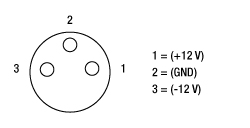
PDB オス型 (電源ケーブル)
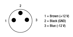
PDB メス型 (フォトディテクタ)
Click to Enlarge
Figure 5.1 当社の15 MHzまでの差分ディテクタのブロック図
使用例:差分ディテクタを使用したドップラーLiDAR
当社製品を使用してドップラーLiDAR(Light Detection and Ranging/光測距)システムを構築する方法を説明いたします。主要なコンポーネントは当社の高利得差分フォトディテクタPDB440Cです。差分ディテクタは一般的に高ノイズのシステムで、信号対雑音比(SNR)が小さくなる用途に使用されます。
差分ディテクタがLiDARに適しているのは、コモンモード除去と50:50カプラからの両出射アーム(下記で説明)の使用により、SNRが改善されるからです。コモンモード除去によりコモンモードノイズが減少し(PDB440Cの場合25 dB以上)、またカプラの一方だけではなく、両出射アームを使用することにより、3 dB高い信号レベルが得られます。
当社の差分ディテクタは、2つの整合性のとれたフォトダイオードと超低雑音高速トランスインピーダンスアンプ(TIA)で構成されています。TIAは2つのフォトダイオードの光電流の差分に比例した出力電圧(RF OUTPUT)を生成します。
Click to Enlarge
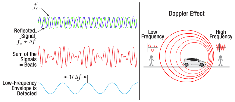
Figure 5.2 ビート周波数の生成(左)とドップラー効果の原理(右)
ドップラーLiDARの理論
電磁波の周波数は移動している物体から反射すると変化します。この変化は一般的にドップラー効果、またはドップラーシフトと呼ばれています。ディテクタの位置が固定されていて、物体が速度vでディテクタの方に向かって移動しているとき、ドップラーシフトΔfは下記のとおり表すことができます。
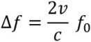
ここで、
c:光の速度(m/s)
f0:光源から放射される光の周波数(Hz)

f1:物体から反射された光の周波数(Hz)です。
当社の差分ディテクタの典型的な波長範囲内では、光の周波数はTHz領域にあり、フォトディテクタで直接記録するには速すぎます。一方で下記の例をご覧ください。

速度0.75 m/s 以下、周波数200 THz、つまり1500 nmの波長に相当することを示すこの例では、ドップラーシフトΔfはkHz領域となり、これは、基準信号からのビート周波数(f0)と、ドップラーシフトした信号(f1)が、標準的なフォトダイオードでも検知可能であることを意味します。異なる2つの周波数の重畳信号を検出することは、ヘテロダイン検出と呼ばれます。
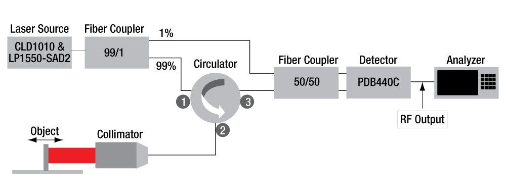
セットアップと原理
基本のコンポーネントは、ファイバ出力レーザと、分岐比99:1のファイバーカプラ、分岐比50:50のファイバーカプラ、ファイバーサーキュレータ、ファイバーコリメータ、差分ディテクタ、高速フーリエ変換機能付きのオシロスコープ、そして速度vで移動する物体です。

Click to Enlarge
Figure 5.3 ブレッドボード上にセットアップしたドップラーLiDARシステム
| Components | Details | |
|---|---|---|
| 1 | Collimator | F810APC-1550 |
| 2 | Light Source | LP1550-SAD2 DFB Laser with Center Wavelength of 1550.1 nm |
| 3 | LD & TEC Driver | CLD1010LP Compact Laser Diode/Temperature Controller |
| 4 | Fiber Coupler (99/1) | TN1550R1A2 |
| 5 | Fiber Coupler (50/50) | TN1550R5A2 |
| 6 | Fiber Circulator | 6015-3-APC |
| 7 | Detector | PDB440C Balanced Photodetector (CMRR > 35 dB; Gain 51 x 103 V/W) |
| Analyzer | Standard Oscilloscope (with 500 kHz Fast Fourier Transform) or Spectrum Analyzer | |
| Object | EDU-VS1/M Viewing Screen, Mounted on DDSM100/M Linear Stage | |
DFBレーザLP1550-SAD2からの光は分岐比が99:1のファイバーカプラにより分岐されています。ファイバーサーキュレータに伝搬した99%の光は、ファイバーコリメータに誘導され、自由空間に出射されます。コリメート光は速度v,で移動する物体に向けられ、反射光がファイバに入力されます。光が戻るとき、サーキュレータは分岐比99:1の1%の方のアームではなく、分岐比50:50のファイバーカプラに誘導します。また、分岐比50:50のカプラのもう一つの入力アームには分岐比99:1の1%の方のアームからの出力光が入射されるため、分岐比50:50のカプラからの出射光は混合の信号が含まれており、その信号が差分ディテクタPDB440Cによって検知されます。
測定と結果
直線ステージは、速度250 mm/sに設定されています。得られる信号は、SNRが10 dB以上の鋭いピークを持ちます。速度は下記の式で計算されます。

直線移動ステージの速度の正確度には、9 mm/s (3.5%)のブレがありますがこれはこの設定で予測される範囲です。
物体は、移動距離100 mmの直線移動ステージDDSM100/Mに置かれています。物体を移動させている間、速度は未知の距離の間一定ではありません。それは直線ステージの加速度は制限されているからです。そのため、信号の周波数は物体が0 mmから100 mmまで移動する間変化します。高速フーリエ変換機能付きのオシロスコープによる1回の測定時間は数十ミリ秒のため、信号の連続変化を観測するのではなく、一定ではない時間間隔での離散的な信号を測定しています。そのため、最大ピークホールド機能を使用して、周波数と物体の最大速度の相関を評価しました。この機能は1回の周波数スキャン中の最大振幅のピークを捉えます。
この使用例では、当社製品を使用したドップラーLiDARの一般的な構成とデモを示しています。ご用途に応じたご質問やご意見について当社までお知らせください。
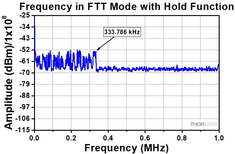
Click to Enlarge
Figure 5.6 オシロスコープの最大ピークホールド機能でFFTモードにおける周波数Δfの測定

Click to Enlarge
Figure 5.5 FFTモードにおける333.786 kHzビート周波数Δfの測定
| Posted Comments: | |
kang wang
(posted 2025-06-03 17:38:57.147) Please provide me with an instruction manual, thank you Taeguk Um
(posted 2024-12-23 12:54:24.547) Hi, my name is Taeguk Um from KASIT in Korea.
I'm reaching for a request about PDB482C-AC
As I know, in Optical Coherence Tomography (OCT) system, length difference between 50:50 coupler ouputs is important to reject high-frequency noise. There is a fiber in each input port inside the PDB482C-AC, so I think this difference in length may have an effect.
Could you please provide information on the manufacturing tolerances associated with the fiber connected to the input port of the PDB482C-AC?
Best regards,
Taeguk Um hkarpenko
(posted 2025-01-03 10:10:48.0) Dear Taeguk,
thank you for your feedback. I will contact you directly regarding this specification. Jerard Vincent Rubio Ang
(posted 2024-11-26 15:01:06.47) We are currently using the balanced detector as for AFM-style measurements, however, we need to calibrate it using an XY stage. As the DC part of the signal is ommited by the RF output, is it okay to calibrate using the monitor outputs? We obtained a conversion factor of around 15 times for the monitor difference vs RF output. hkarpenko
(posted 2024-11-27 09:07:34.0) Dear customer,
thank you for your feedback. I will contact you directly to discuss this issue further with you. user
(posted 2024-11-06 10:00:16.86) Hello,
We have the PDB425A and we were wondering which acquisition card is recommended to digitize the acquired OCT signal ? jjadvani
(posted 2024-11-11 04:22:05.0) Dear User, Thank you for the feedback. This PDB has a bandwidth of 75 MHz, and to adequately resolve this frequency, I would consider using a DAQ with double frequency (150 Msample/s). A higher sample rate would also be beneficial. Regarding the voltage input, you may determine the output voltage for your signal by taking the detector's TIA and the input current. I would suggest +/- 5 to +/-10 V is a good choice. Any DAQ card that meets these requirements can be used. user
(posted 2024-07-31 12:51:29.13) For the PDB835 on the specs tab, RF OUTPUT CW Saturation Power should have units of microWatts, right? jjadvani
(posted 2024-08-01 02:46:18.0) Dear user, Thank you for providing feedback. The PDB835 has an RF output CW saturation power of 360 µW at 1550 nm. There is a typo in the spec table, which we will fix soon. Jerard Vincent Rubio Ang
(posted 2024-05-17 19:28:22.223) What size screws are used on the FC adapter? We lost some of the screws for ours. jjadvani
(posted 2024-05-17 08:30:39.0) Dear Jerard, Thank you for your feedback. The size of the screw for FC fiber input holder is M2 x 4 Allen screw. Jaeyoon Ko
(posted 2024-03-06 15:58:04.61) Dear Thorlabs Team, Hello! I'm recently recieved your PDB425A-AC and tried to use for balanced photodetection in pump-probe setup. I am using femtosecond 520 nm laser. My probe beam reflects from the sample and enters Input + and planning to induce sampled probe beam to Input - port.
However, there are some phase difference between two inputs. When I induce probe beam and view through oscilloscope(triggered by laser source internal oscillator), there are 5 ns of phase difference. Is this normal? dpossin
(posted 2024-03-06 08:40:59.0) Dear Yaeyoon,
Thank you for your feedback. A possible reason for a phase difference could be that the optical path lengths are not equal. You can view the optical path length difference vs frequency shift on the PDB manual in section 3.7. One method in order to compensate for that is to use an optical delay line.
I reach out to you directly to discuss your application in more detail.
Best regards,
Dominik Kye Kwanuk
(posted 2024-02-04 22:54:59.377) Hello. I'm interested in Thorlabs's doppler lidar detector, PDB series.
I was looking for some doppler lidar publications, and many publications used PDB430C-AC detector from Thorlabs. but PDB430C-AC is obsoleted, and it seems that PDB435C-AC has simillar spec.
My question is that,
Is PDB435C-AC an upgraded version of product PDB430C-AC? or are they just seperated products?
Thanks hkarpenko
(posted 2024-02-07 02:54:18.0) Dear customer,
thank you for your feedback. We use a revised photodiode of the same model for this new balanced detector. The specifications are very similar to the obsolete version, as you already mention. I will contact you directly to discuss your application in detail and help you choosing the correct detector. Nikita Kikilich
(posted 2023-12-12 09:49:44.517) Hello! We are using PDB470C-AC for measurement application. We are faced with a problem that is very similar to restoring a photodetector after a strong signal. Could you give us additional information about the model of the photodetector (the PIN diode itself) or at least its capacity, saturation threshold, and so on. dpossin
(posted 2023-12-13 09:20:55.0) Dear Nikita,
Thank you for your feedback. I reach out to you in order to provide the requested details. dpossin
(posted 2023-12-13 09:20:55.0) Dear Nikita,
Thank you for your feedback. I reach out to you in order to provide the requested details. Markus Schmit
(posted 2023-10-07 13:23:45.87) Dear Thorlabs team! Thank you very much for your explanation about Homodyne detectors. I have a PDB425C-AC detector and would like to ask you about laser power applied to this detector in my setup. According to its datasheet, it's said that to avoid saturation in Monitors and to prevent nonlinearities in RF output, the input power should be less than 1mW and 4W/cm2, respectively. Are they DC power or peak power?
Many thanks and best regards, Markus. hkarpenko
(posted 2023-10-12 04:09:39.0) Dear Markus,
thank you for your kind feedback. In general these values are tested for a CW input. We have not tested the saturation power for pulsed sources, thus I would expect the threshold value to be a little higher. For your application I would recommend to start with a value below 1mW peak power and slightly increase it until you see saturation on the detector. That way you will avoid damage to the amplifier. The maximum damage threshold of the photodiode is 20mW (CW and peak power). Exceeding this value will permanently damage the detector. Semyon Vasilchenko
(posted 2023-05-29 10:14:21.317) Dear Sir or Madam, Monitor channel Transimpedance Gain is not given in specs. Do I properly calculate it for PDB450C as 10000 V/W since Max Responsivity for a photodiode is given as 1.0 A/W and Conversion gain is 10 V/mW @ 1550 nm? If I'm wrong please tell me Monitor Output Transimpedance Gain. hkarpenko
(posted 2023-05-31 06:05:40.0) Dear customer,
thank you for your feedback. Indeed, you did calculate it correctly by using the responsivity a conversion gain CG. The TIA gain is 10^4 V/A of the monitor port. William P
(posted 2023-03-07 15:32:37.563) Dear Thorlabs,
I very much appreciate your explanations and application ideas. Regarding Doppler lidar, I have a simple (maybe naive) question: I understand that using a balanced detector can significantly reduce common noise, but does the useful beat signal also decrease due to the difference in photocurrents between the two photodiodes? Thank you in advance.
William hkarpenko
(posted 2023-03-09 11:05:27.0) Dear William,
thank you very much for your kind feedback.
The beat signal will not be decreased, since it will only be present on one of the two photodiodes. I will contact you directly to discuss this further with you. Vladimir Zenin
(posted 2023-02-08 15:27:29.193) Dear Thorlabs,
I would like to ask your advice regarding the noise. In my setup I need to measure small modulations on top of a large nearly-DC signal, therefore I have kind of lock-in setup. Here is what I noticed: even when I have no modulations, and light comes directly to the detector, there is a signal (noise) produced by lock-in. And this noise is proportional to the optical power. Is this noise somehow related to NEP, or is it a different specification of the detector? I always though NEP is a noise with no optical power hitting the detector. Also, about my case, I have balanced detectors PDB450A and PDB450C, and I can verify that the noise I see is not from the laser (the noise is present in RF output, and doesn't change after unbalancing the detector). If you have any suggestions for a different detector for my setup, it is more than welcome :) Thank you in advance! dpossin
(posted 2023-02-14 04:47:36.0) Dear Vladimir,
Thank you for your feedback. I am looking into this. I am reaching out to you directly in order to discuss it in more detail. Vladimir Zenin
(posted 2023-01-11 17:02:31.933) Dear Thorlabs,
My question is about switchable-gain detector PDB450A-AC. In specs it says CW Saturation Power RF Output 9 mW, which, probably, produces 10V at RF output at lowest gain. However, and this power Monitors will be way beyond saturation (their gain is 10 V/mW, and max 10V output). I am wondering, is it ok to operate the detector with saturated monitors, but when RF output is below saturation (i.e., with 9 mW of optical power)? If not, what is the upper limit for normal operation? Thank you in advance!
P.S. I have both PDB450A and PDB450C detectors - very satisfied with them! hkarpenko
(posted 2023-01-12 07:59:24.0) Dear Vladimir,
thank you for your kind feedback. You are correct, the CW saturation power of the RF output is 9mW, while the saturation power of the monitor ports is only 1mW according to the spec sheet.
I will contact you directly to discuss this issue further with you. user
(posted 2022-12-28 17:02:50.843) When I connect the Monitor output+ to an oscilloscope for 50 ohm load and connect the RF output for 50 ohm load also, the amplitude of RF output was about 15-times-larger than Monitor output's one.
The Conversion Gain of RF and Monitor output for 50 ohm load are 25V/mW and 10V/mW, respectively, so I expected that the output of RF becomes 2.5-times-larger than that of Monitor.
What causes this? dpossin
(posted 2022-12-28 06:41:21.0) Dear Hiroki,
Thank you for your feedback. The main difference between the RF output and the monitor output is the bandwidth. For the PDB415C the bandwidth of the RF output is 100MHz while the bandwidth for the monitor outputs is limited to 1MHz. The main purpose of the monitor outputs is alignment. Since they show crosstalk too they are not well suited for the actual balanced measurement. I am reaching out to you in order to dig in in more detail. Megha Jain
(posted 2022-09-29 10:57:42.717) I want to know the rise time of detector. hkarpenko
(posted 2022-09-29 08:36:45.0) Dear Megha,
thank you for your feedback.
The risetime of a detector can be calculated from the bandwidth according to this formula: risetime = 0.35/bandwidth. The PDB425A has a maximum bandwidth of 75MHz, which corresponds to a risetime of 4.7ns. I contact you directly to discuss this further with you. Felix B
(posted 2022-02-23 07:08:29.95) Dear Sir or Madam,
I have the PDB450C detector and have unscrewed the fibre holders. Now I would like to attach a (self constructed) mount for a lens (e.g. LA1540-C) to the attached four threads. For this I need the distance of the active surface of the photodiodes to a reference plane. Could you tell me this distance? Unfortunately, I did not find this information in the data sheet.
It would also be interesting to know the tolerances with which the photodiodes are mounted.
Best regards, Felix dpossin
(posted 2022-02-23 10:50:04.0) Dear Felix,
Thank you for your feedback. The distance between the coverglass of the photodiode and the fiber tip is 0.4 +/- 0.05mm. I am reaching out to you to discuss this in more detail. Jameel Ali
(posted 2021-12-14 06:49:39.44) Dear Sir/Madam,
We have an optical fiber sensing experiment aimed to sense vibration signals or events. In our experiment, se send a laser at 1550nm through the fiber, and that laser wave will be picking the phase /amplitude variations in the fiber. And at the end of the fiber, we want to use a photodetector that can detect the signals.
Our vibration signal has low bandwidth (few Hz - tens of kHz). In addition, the received optical power in our experimental setup is very low ( in the range of -xx.x dBm). Therefore, we would like you please to recommend a suitable photodiode/photoreceiver model to help us in our application. soswald
(posted 2021-12-17 06:53:07.0) Dear Jameel,
thank you for your feedback. I have reached out to you directly to discuss your application in more detail. Aleksey Lopatin
(posted 2021-09-29 10:21:12.447) Dear Sir/Madam,
How do you define SMRR for PDB425A? (I've bought one already).
As SMRR=10log(V1/V2) or SMRR=20log(V1/V2). Speaking about voltage output, it should be SMRR=20log(V1/V2). However, in some literature, related to balanced photodetectors, one can find definition SMRR=10log(I1/I2).
What is your SMRR definition?
Regards,
Aleksey dpossin
(posted 2021-10-06 08:25:27.0) Dear Aleksey,
Thank you for your feedback. We measure the CMRR with a network analyzer. Therefore we use a laser modulated by the network analyzer and splitted into two path with a 3dB fusion coupler such that the path length difference is as small as possible. Both branches of the coupler output are connected to the input ports of the PDB. On the other side the RF output of the PDB is connected to the measurement port of the networt analyzer. The difference between both inputs and the balanced signal at the 3 dB frequency means the CMRR value. Please also see a more detailed explanation in the PDB manual: https://www.thorlabs.de/thorproduct.cfm?partnumber=PDB425A user
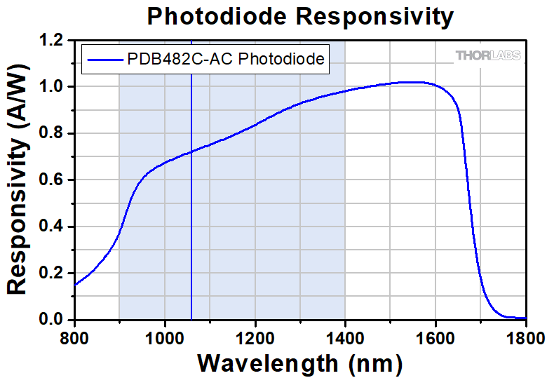
(posted 2021-08-31 07:24:27.86) The typical detector responsivity curve shows that the detector is still responsive to light at 1600 nm, but why the working wavelength (shaded area) can only reach 1400 nm dpossin
(posted 2021-09-07 10:13:36.0) Dear customer,
Thank you for your feedback. The graph shows the responsivity of the photodiodes inside the PDB482C-AC but the usable working range is limited by the fiber which connects the fiberports to the photodiodes. The highlighted intersection represents the working range. I am reaching out to you to discuss this further. David shoala
(posted 2021-08-09 13:16:55.207) Hello
I'm David
I hope you are well
We have already one Balanced Detector from your company( model: PDB470c )
Unfortunately Carelessly we were working with a 20mW CW laser for 1 minute permanently after that one of two detectors doesn’t have any response on an oscilloscope.
Is that detector is destroyed ??
If yes but I have a question about photodiode
Is this photodiode replaceable?
How to repair this balanced detector
Best regards
David dpossin
(posted 2021-08-09 07:35:47.0) Dear David,
Thank you for your feedback. Since the damage threshold has been exceeded most probably the photodiode which has been exposed is damaged now. However we can replace the damaged photodiode via RMA. I am reaching out to you in order to provide further details on the process. Minsuk Lee
(posted 2021-05-24 18:36:11.37) We are currently using a PDB465C for an 1300nm SSOCT application.
We need a response time to correctly select k-trigger delay time.
Can you tell me what the response time is? MKiess
(posted 2021-05-27 09:07:39.0) This is a response from Michael at Thorlabs. Thank you very much for your inquiry. The rise time of the balanced output signal can be calculated from the signal bandwidth using this formula: Rise time = 0.35 / Bandwidth. The bandwidth of the PDB465C is 200 MHz. This corresponds to a rise time of 1.75 ns I will contact you directly to provide further assistance. 陈 潜源
(posted 2021-05-21 11:37:03.35) 我们有个在您们公司买的类似这款探测器,S/N.:M00319347。现在我想要他的说明书和规格参数,请问您们能发送到我的邮箱吗? YLohia
(posted 2021-05-24 10:37:44.0) Thank you for contacting Thorlabs. We will reach out to you directly. Seth Erickson
(posted 2020-10-26 14:52:00.707) On the PDB415A, the two photodiodes are mounted 20 mm apart. While this is fine for fiber coupled operation, it creates a problem for free space coupling. Since we use 1 inch optics with 1/2" posts & post holders, it is actually impossible to get proper lens alignment, since having the center of the lenses 20 mm apart results in overlapping lenses. Since this is a common lab setup, it seems silly that the photodiodes are 20 mm apart instead of 30-35 mm, which would provide 5-10 mm separation between lenses, allowing room for pedestal mounting. Might be a silly nitpick, but thought you might appreciate the feedback. Cheers MKiess
(posted 2020-10-27 10:26:35.0) Dear Seth, Thank you very much for this feedback. This is not a silly nitpick. Such feedback helps us to constantly improve our products. Even though the PDB415A is mainly designed for fiber applications, it is also suitable for free space applications due to the possible removal of the FC adapter. Therefore, it is correct that the distance is not ideal for a free space application with the standard sizes, 1/2" or 1" optics. Thank you very much for this information. For applications with larger optics the detector you can find under the following link would be more suitable:
https://www.thorlabs.de/newgrouppage9.cfm?objectgroup_id=1299&pn=PDB210A Qiangzhou Rong
(posted 2020-06-17 09:13:10.84) Dear Mr/Mrs/Miss,
I am postdoc at Duke University. We bought a PDB425C-AC detector recently. The noise from the RF port is larger than 100 mV without any light input. It is too large to be used in experiment. Is it correct or something rong in operation make it so large? Could you give me some comments as soon as possible? Urgently waiting for kind help! Thank you very much!
Best regards,
Qiangzhou Rong MKiess
(posted 2020-06-19 07:31:15.0) This is a response from Michael at Thorlabs. Thank you for the inquiry.A noise of more than 100mV is too high for this detector, if used properly. I have contacted you directly to discuss your application and find a solution together with you. wu nigel
(posted 2020-02-05 17:39:41.227) please tell me Balanced detector life MKiess
(posted 2020-02-06 06:18:35.0) This is a response from Micael at Thorlabs. Thank you for the inquiry. I have contacted you directly to discuss the influences on the lifetime of the detector in relation to your application. Kristof Reynkens
(posted 2019-06-27 05:02:47.707) I wondered if the PDB450A(-AC) can be cooled and how the NEP would change vs temperature. dpossin
(posted 2019-06-28 09:57:23.0) Hello Kristof,
Thank you for your Feedback. In general the NEP will decrease when you lower the temperature. The NEP with respect to wavelength can be calculated the following way: NEP(lambda)=(R_max/R(lambda))x NEP_min.
There R_max is the maximum responsivity, R(lambda) is the responsivity with respect to the wavelenght and NEP_min is the NEP value which is specified on the homepage.
The detector can be cooled but you will need to build up the cooling circuit yourself.
I will reach out directly to you to support you with temperature related data on the photodiode itself. Jonathan Doorn
(posted 2019-04-01 18:34:40.513) I am running some noise experiments with this device, the PDB450A, and I would like to know more about the noise characteristics of this device. What opamps does this device use? swick
(posted 2019-04-05 03:46:29.0) This is a response from Sebastian at Thorlabs. Thank you for the inquiry. In the manual we show graphs with typical spectral noise for PDB450A at each gain setting. I contacted you directly to provide further assistance. zenin
(posted 2019-02-20 10:03:49.533) Hi,
Currently I am using PDB450C and PDB450A-AC. I found that AC-coupled detection is better for my setup, so I am wondering, is it possible to upgrade my PDB450C to AC-coupled version? If yes, what is time scale and price?
Additionally, I would like to give you two proposals for making it better:
1) It would be nice to have a single device with on-off switch for AC-coupling. Then people like me would not make trials & errors on which one to buy.
2) The holder for post-mounting (with 4 holes to attach to detector) is rather disappointing. It seems to be made of plastic, and one cannot screw it tight. You see, I am using both VIS and NIR detectors for free-space beams, and I wanted to attach each BD to magnetic mount in order to have fast switch, when I change the source. The light is focused by two parabolic mirrors, and there are two precision translation 3D stages, so I wanted to not buy and build separate sets of those for each BD. But mounting of BD to magnetic mount was a nightmare: 4 holes in BD are not standart-size (I would prefer separation of 2.5 cm or separation like for the cage system). I hope that in future you will make this mount better and compatible with standart Thorlabs dimensions.
Best,
Vladimir nreusch
(posted 2019-02-27 01:55:14.0) This is a response from Nicola at Thorlabs. Thank you for your good suggestions! We will take them into account in the future. We can also offer to upgrade the PDB to the -AC version. I will contact you directly with further information. Carsten.Kuehn
(posted 2018-01-08 18:36:56.437) In your Datasheet the PDB415C is speced for tempertures upto 40degC.
What will happen when the amplifier is used at higer temperatures?
Is there a high temperature version of this amplifier, which is able to operate at 75degC ambient.
Thanks in advance! swick
(posted 2018-01-12 03:21:02.0) This is a response from Sebastian at Thorlabs. Thank you for the inquiry. All specified parameters for PDB415C can not be guaranteed when used outside of operating temperature range. At 75°C the detector should still work but performance will be worse. We do not offer high-temperature versions for this detector. gregory.gaeumann
(posted 2017-06-23 09:50:38.3) What's the rise time of the balanced output signal of PDB450A(-AC)? wskopalik
(posted 2017-06-23 10:17:58.0) This is a response from Wolfgang at Thorlabs. Thank you very much for your inquiry.
The rise time of the balanced output signal can be calculated from the signal bandwidth using this formula: Rise time = 0.35 / Bandwidth.
The bandwidth of the PDB450A / PDB450A-AC is in the range of 0.1 - 150 MHz depending on the gain setting. This corresponds to rise times of 3.5 µs at 0.1 MHz and 2.3 ns at 150 MHz.
I will contact you directly to provide further assistance. john_noriega
(posted 2016-11-22 15:12:31.733) Can you please clarify the spec "CW Saturation Power RF-Output" Is that the optical power that will saturate the RF output, or is that the optical power that saturates the photodiode, thus limiting the RF output? Or am I missing some other interpretation? swick
(posted 2016-11-23 04:56:10.0) This is a response from Sebastian at Thorlabs. Thank you very much for the inquiry.
The parameter "CW Saturation Power RF-Output" is referred the power difference between the optical inputs. This value must not be exceeded to prevent saturation of the balanced amplifier, which would cause nonlinear behavior.
Saturation of the Monitor outputs will occur at optical input power levels greater than 1 mW.
You can find this explanation in the manual at Chapter 3. mahldyla
(posted 2015-02-27 11:42:57.35) To whom it may concern: Could you explain how the plots of "spectral noise" and "frequency response" are measured for each of the balanced detectors? The reason that I ask is that, with balanced inputs, the output should be shot noise, which is white. I would expect both plots to be identical then, if I am not misunderstanding anything. Also, is there a way to flatten the frequency response of the detector? tschalk
(posted 2015-03-03 10:15:39.0) This is a response from Thomas at Thorlabs. Thank you very much for your inquiry. Please note that the measurement of "spectral noise" and "frequency response" is explained in the manual of the PDBs: http://www.thorlabs.de/thorcat/21600/PDB450C-AC-Manual.pdf. You can find the information you are looking for at section 3.6 CMRR and Frequency Response and at section 5 Appendix Typical noise spectra. Unfortunately, it is not possible to flatten the frequency response. I will contact you directly with more detailed information. kiwa
(posted 2015-01-08 04:02:02.833) What is the rise and fall time of the PDB410A?
I want to use it together with Maitai Ti:sapphire oscilator at 42 MHz together with boxcar which will sellect one pulse at 1kHz rate for THz detection via balanced detection.
I'm wondering if 100 MHz diodes are fast enough, or shall I go for 350 MHz?
It is a free space optics setup so it's better if photodiodes have large area. shallwig
(posted 2015-01-09 03:40:54.0) This is a response from Stefan at Thorlabs. Thank you very much for your inquiry. You can calculate the rise time of the PDB410A by using the specified 3dB bandwidth and the following formula: f(3dB)=0.35/rise time. This gives you a rise time of 3.5ns. This limitation comes from the built in amplifier. I will contact you directly to discuss your application in detail and to check which PDB meets your requirements best. bpursley
(posted 2014-12-29 12:40:43.14) To whom it may concern:
Do you have a model (or could suggest one) for the frequency response of the various gain settings on the PDB450A? In particular, the 10^3 and 10^4 gain settings? Thanks in advance! shallwig
(posted 2015-01-07 04:59:03.0) This is a response from Stefan at Thorlabs. Thank you very much for your inquiry. We specify the frequency response for various gain settings in the spec sheet of the PDB450A as follows:
RF OUTPUT Bandwidth (-3 dB): DC - 150 / 45 / 4 / 0.3 / 0.1 MHz
RF OUTPUT Transimpedance Gain: 10^3 / 10^4 / 10^5 / 10^6 / 10^7 V/A
So for 10^3 and 10^4 gain settings the 3dB bandwidth is specified with DC-150MHz and DC-45MHz . In the manual http://www.thorlabs.com/thorcat/21600/PDB450A-Manual.pdf on page 31 you can also find a curve showing the frequency versus amplitude for the different gain settings.
I will contact you directly to discuss your application in detail and to check if you need further information. bdada
(posted 2011-12-29 11:27:00.0) Response from Buki at Thorlabs:
To keep everything free-space, I would recommend post mounting two mirrors to an optical table. To minimize space requirements, one of the mirrors can be D shaped. We have sent you a schematic describing the set up.
Unfortunately there is not an easy way to mount a lens directly to the balanced detector box.
Please contact TechSupport@thorlabs.com if you have any questions. boris.povazay
(posted 2011-12-27 16:24:59.0) Dear Thorlabs team!
You mention that free-space coupling onto the detectors is possible with by dismounting the FC-connectors. However - it is unclear how to couple into that 0.8-0.3mm wide detectors. Especially since they are so close together it is extremely challenging to hit them with a focussed beam. Do you have any suggestions up your sleeve on how to mount pair of lenses with x-y-z positioning capability to the detector box (rather than independently in front of the device)?
Many thanks and best regards,
Boris jvigroux
(posted 2011-12-05 09:53:00.0) A response from Julien at Thorlabs: the distance between the photodiode chip and the ferrule of the fiber is between 600µm and 1.1mm. This range is the sum of the mechanical tolerances given by the photodiode manufacturer and ours. user
(posted 2011-11-30 15:31:01.0) A response from Tyler at Thorlabs to Sergey: The diameter of the photodiodes is 0.8 mm. We are looking into the distance between the fiber tip and the photodiode. We will contact you with this information and help you determine an appropriate fiber. Sergey.L.Vinogradov
(posted 2011-11-29 01:14:37.0) Dear support staff,
I try to use PDB450A in Dynamic Light Scattering Spectroscopy at 633 nm with various MM fiber core diameter ranging from 50 to 400 um. Regretfully, I did not find any information on alignment of FC receptacle to photodiode except some general remark:
"In general, multi-mode fiber at the input can be used, but in this case the light beam
spot diameter exceeds detector’s active area, which results in a reduced output
signal as well."
Nevertheless, I assume that some large core fiber with low NA could be coupled to photodiode aperture without losses.
Please, let me see some mechanical drawing related to that, at least clarifying the distance between receptacle and photodiode. I would also appreciate your advises on appropriate combination of NA and core diameter providing lossless coupling.
Thanks in advance,
Sergey Vinogradov jvigroux
(posted 2011-06-06 08:17:00.0) A response from Julien at Thorlabs: Dear Claudius, the bandwidth of the monitor outputs is unfortunately limited by the amplifier that is used for those. An upgrade up to 100MHz or higher is of course technically possible but would imply a large amount of modification and would probably driver the price up substantially. Should you be interested anyways, please contact our technical support at techsupport@thorlabs.com weimann
(posted 2011-06-03 06:59:44.0) Dear Sir or Madam,
Is there the possibility to get a balanced detector with an even faster monitor output?
For a current research project a balanced detector with the possbibility to read out a ~100 MHz (or faster) signal from the single PDs would be really helpful.
Yours sincerely,
Claudius Weimann. |

 ズーム
ズーム| Specificationsa | ||||
|---|---|---|---|---|
| Item # | PDB450A(-AC) | PDB450C(-AC) | ||
| Detector Type | Si/PIN | InGaAs/PIN | ||
| Wavelength Range | 320 - 1000 nm | 800 - 1700 nm | ||
| Max Responsivity (Typical) | 0.53 A/W | 1.0 A/W | ||
| Active Detector Diameter | 0.8 mm | 0.3 mm | ||
| Bandwidth (3 dB) | DC - 150, 45, 4, 0.3, 0.1 MHz AC Coupled (-AC Suffix): 100 Hz - 150, 45, 4, 0.3, 0.1 MHz | |||
| Common Mode Rejection Ratio | > 25 dB | |||
| Transimpedance Gainb | 103, 104, 105, 106, 107 V/A | |||
| Minimum NEP | DC - 0.1 MHz: 1.4 pW/Hz1/2 DC - 0.3 MHz: 1.1 pW/Hz1/2 DC - 4.0 MHz: 3.3 pW/Hz1/2 DC - 45 MHz: 28.9 pW/Hz1/2 DC - 150 MHz: 123 pW/Hz1/2 | DC - 0.1 MHz: 0.7 pW/Hz1/2 DC - 0.3 MHz: 0.5 pW/Hz1/2 DC - 4.0 MHz: 1.55 pW/Hz1/2 DC - 45 MHz: 14.9 pW/Hz1/2 DC - 150 MHz: 68.6 pW/Hz1/2 | ||
| Optical Inputs | FC/PC or FC/APC Compatible (Removable Adapter) | |||
| Monitor Output Bandwidth | DC - 1 MHz | |||


 ズーム
ズーム| Specificationsa | ||||
|---|---|---|---|---|
| Item # | PDB440A(-AC) | PDB440C(-AC) | ||
| Detector Type | Si/PIN | InGaAs/PIN | ||
| Wavelength Range | 320 - 1000 nm | 800 - 1700 nm | ||
| Max Responsivity (Typical) | 0.53 A/W | 1.0 A/W | ||
| Active Detector Diameter | 0.8 mm | 0.3 mm | ||
| Bandwidth (3 dB) | DC - 15 MHz AC Coupled (-AC Suffix): 100 Hz - 15 MHz | |||
| Common Mode Rejection Ratio | > 35 dB | |||
| Transimpedance Gainb | 51 x 103 V/A | |||
| Minimum NEP | 6.9 pW/Hz1/2 (DC - 15 MHz) | 3.9 pW/Hz1/2 (DC - 15 MHz) | ||
| Optical Inputs | FC/PC or FC/APC Compatible (Removable Adapter) | |||
| Monitor Output Bandwidth | DC - 1 MHz | |||

 ズーム
ズーム| Specificationsa | ||
|---|---|---|
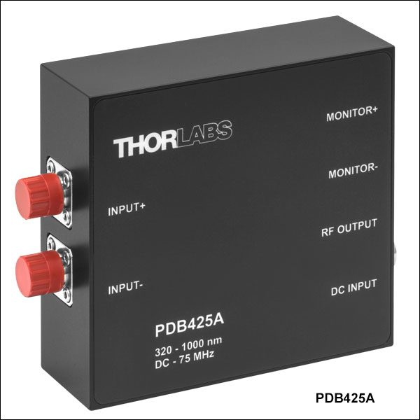
| Item # | PDB425A(-AC) | PDB425C(-AC) |
| Detector Type | Si/PIN | InGaAs/PIN |
| Wavelength Range | 320 - 1000 nm | 800 - 1700 nm |
| Max Responsivity (Typical) | 0.53 A/W | 1.0 A/W |
| Active Detector Diameter | 0.8 mm | 0.3 mm |
| Bandwidth (3 dB) | DC - 75 MHz AC Coupled (-AC Suffix): 100 Hz - 75 MHz | |
| Common Mode Rejection Ratio | > 35 dB | |
| Transimpedance Gainb | 250 x 103 V/A | |
| Minimum NEP | 9.5 pW/Hz1/2 (DC - 75 MHz) | 5.2 pW/Hz1/2 (DC - 75 MHz) |
| Optical Inputs | FC/PC or FC/APC Compatible (Removable Adapter) | |
| Monitor Output Bandwidth | DC - 1 MHz | |


 ズーム
ズーム| Specificationsa | ||
|---|---|---|
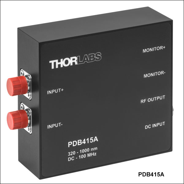
| Item # | PDB415A(-AC) | PDB415C(-AC) |
| Detector Type | Si/PIN | InGaAs/PIN |
| Wavelength Range | 320 - 1000 nm | 800 - 1700 nm |
| Max Responsivity (Typical) | 0.53 A/W | 1.0 A/W |
| Active Detector Diameter | 0.8 mm | 0.3 mm |
| Bandwidth (3 dB) | DC - 100 MHz AC Coupled (-AC Suffix): 100 Hz - 100 MHz | |
| Common Mode Rejection Ratio | > 25 dB | |
| Transimpedance Gainb | 50 x 103 V/A | |
| Minimum NEP | 12.03 pW/Hz1/2 (DC - 100 MHz) | 6.99 pW/Hz1/2 (DC - 100 MHz) |
| Optical Inputs | FC/PC or FC/APC Compatible (Removable Adapter) | |
| Monitor Output Bandwidth | DC - 1 MHz | |


 ズーム
ズーム| Specificationsa | ||
|---|---|---|
| Item # | PDB465A(-AC) | PDB465C(-AC) |
| Detector Type | Si/PIN | InGaAs/PIN |
| Wavelength Range | 320 - 1000 nm | 800 - 1700 nm |
| Max Responsivity (Typ.) | 0.50 A/W | 1.0 A/W |
| Active Detector Diameter | 0.8 mm | 0.15 mm |
| Bandwidth (3 dB) | DC - 200 MHz AC Coupled (-AC Suffix): 100 Hz - 200 MHz | |
| Common Mode Rejection Ratio | > 25 dB | |
| Transimpedance Gainb | 30 x 103 V/A | |
| Minimum NEP | 22.86 pW/Hz1/2 (DC - 200 MHz) | 8.52 pW/Hz1/2 (DC - 200 MHz) |
| Optical Inputs | FC/PC or FC/APC Compatible (Removable Adapter) | FC/PC or FC/APC Compatible (Adapter is not Removable) |
| Monitor Output Bandwidth | DC - 1 MHz | |


 ズーム
ズーム| Specificationsa | ||
|---|---|---|
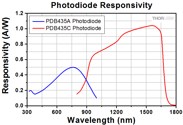
| Item # | PDB435A(-AC) | PDB435C(-AC) |
| Detector Type | Si/PIN | InGaAs/PIN |
| Wavelength Range | 320 - 1000 nm | 800 - 1700 nm |
| Max Responsivity (Typ.) | 0.50 A/W | 1.0 A/W |
| Active Detector Diameter | 0.4 mm | 0.15 mm |
| Bandwidth (3 dB) | DC - 350 MHz AC Coupled (-AC Suffix): 100 Hz - 350 MHz | |
| Common Mode Rejection Ratio | > 20 dB | |
| Transimpedance Gainb | 10 x 103 V/A | |
| Minimum NEP | 32.3 pW/Hz1/2 (DC - 350 MHz) | 15.28 pW/Hz1/2 (DC - 350 MHz) |
| Optical Inputs | FC/PC or FC/APC Compatible (Removable Adapter) | FC/PC or FC/APC Compatible (Adapter is not Removable) |
| Monitor Output Bandwidth | DC - 1 MHz | |

 ズーム
ズーム| Specificationsa | ||
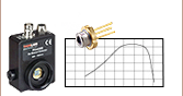
|---|---|---|
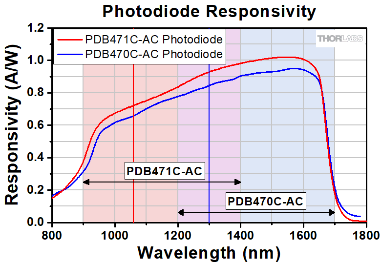
| Item # | PDB471C(-AC) | PDB470C(-AC) |
| Operating Wavelength | Optimized for 1060 nm (900 - 1400 nm Range) | Optimized for 1300 nm (1200 - 1700 nm Range) |
| Detector Type | InGaAs/PIN | |
| Internal Coupling Fiber | HI1060 | SMF-28e+ |
| Responsivity (Typical) | 0.72 A/W @ 1060 nm | 0.9 A/W @ 1550 nm |
| Active Detector Diameter | 0.080 mm | 0.075 mm |
| Bandwidth (3 dB) | DC - 400 MHz AC Coupled (-AC Suffix): 100 Hz - 400 MHz | |
| Common Mode Rejection Ratio | > 25 dB (Typ. > 30 dB) | |
| Transimpedance Gainb | 10 x 103 V/A | |
| Minimum NEP | 8 pW/Hz1/2 (DC to 100 MHz) | |
| Optical Inputs | FC/APC | |
| Monitor Output Bandwidth | DC - 3 MHz | |
Click to Enlarge
2本の縦線はそれぞれ1060 nm (赤)と1300 nm (青)を示しています。網掛けの部分は各ディテクタの仕様波長を示しています。

 ズーム
ズーム| Specificationsa | |
|---|---|
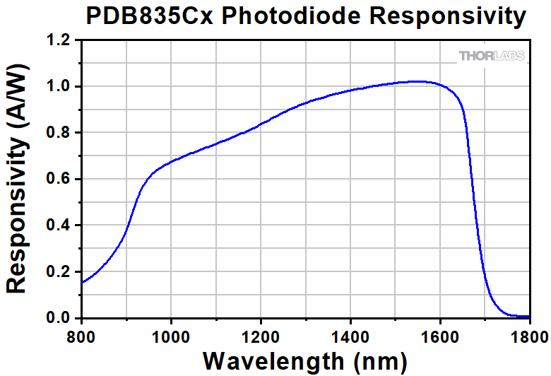
| Item # | PDB835C(-AC) |
| Detector Type | InGaAs/PIN |
| Wavelength Range | 800 - 1700 nm |
| Max Responsivity (Typical) | 1.0 A/W @ 1550 nm |
| Active Detector Diameter | 0.08 mm |
| Bandwidth (3 dB) | DC - 500 MHz AC Coupled (-AC Suffix): 1 kHz - 500 MHz |
| Common Mode Rejection Ratio | > 25 dB |
| Transimpedance Gainb | 10 x 103 V/A |
| Minimum NEP | 6.5 pW/Hz1/2 (DC to 500 MHz) |
| Optical Inputs | FC/APC |
| Monitor Output Bandwidth | DC - 1 MHz |

 ズーム
ズーム| Specificationsa | ||
|---|---|---|
| Item # | PDB481C-AC | PDB480C-AC |
| Operating Wavelength | Optimized for 1060 nm (900 - 1400 nm Range) | Optimized for 1300 nm (1200 - 1700 nm Range) |
| Detector Type | InGaAs/PIN | |
| Internal Coupling Fiber | HI1060 | SMF-28e+ |
| Responsivity (Typical) | 0.72 A/W @ 1060 nm | 0.9 A/W @ 1550 nm |
| Active Detector Diameter | 0.080 mm | 0.075 mm |
| Bandwidth (3 dB) | 30 kHz - 1.0 GHz | 30 kHz - 1.6 GHz |
| Common Mode Rejection Ratio | > 25 dB (Typ. > 30 dB) | |
| Transimpedance Gainb | 16 x 103 V/A | |
| Minimum NEP | 9.0 pW/Hz1/2 (30 kHz to 100 MHz) | 9.3 pW/Hz1/2 (30 kHz to 100 MHz) |
| Optical Inputs | FC/APC | |
| Monitor Output Bandwidth | DC - 3 MHz | |

Click to Enlarge
2本の縦線はそれぞれ1060 nm (赤)と1300 nm (青)を示しています。網掛けの部分は各ディテクタの動作波長範囲を示しています。

 ズーム
ズーム| Specificationsa | |
|---|---|
| Item # | PDB482C-AC |
| Operating Wavelength | Optimized for 1060 nm (900 - 1400 nm Range) |
| Detector Type | InGaAs/PIN |
| Internal Coupling Fiber | HI1060 |
| Responsivity (Typical) | 0.72 A/W @ 1060 nm |
| Active Detector Diameter | 0.080 mm |
| Bandwidth (3 dB) | 1 MHz - 2.5 GHz |
| Common Mode Rejection Ratio | > 20 dB (> 25 dB Typ.) |
| Transimpedance Gainb | 28 x 103 V/A |
| Minimum NEP | 12.0 pW/Hz1/2 (1 MHz to 100 MHz) |
| Optical Inputs | FC/APC |
| Monitor Output Bandwidth | DC - 2.5 MHz |
Click to Enlarge
縦線はディテクタの最適波長(1060 nm)、網掛けの部分は動作波長範囲を示しています。

 ズーム
ズーム Figure 508A 電源ケーブルLDS12B
- 差分増幅フォトディテクタ(上記掲載)の交換用電源
- ±12 VDC出力
- 短絡回路を保護しオーバーロードを防ぐ電流リミット機能
- LED表示付きのOn/Offスイッチ
- AC入力電圧はスイッチ切り替え可能(100/120/230 VAC)
- 長さ2 mのケーブル、LUMBERG製オス型コネクタRSMV3付き
この±12 VDC安定化リニア電源LDS12Bは、上記掲載のPDBシリーズの差分フォトディテクタに付属する電源の交換用製品です。ケーブルに付いているコネクタは3ピンで、グランド用、+12 V用、-12 V用となっています(Figure 508A参照)。また、日本国内仕様の電源ケーブルが付属します。この電源は当社のPDAシリーズの増幅ディテクタ、PMMシリーズの光電子増倍管モジュールAPDシリーズのアバランシェフォトディテクタ、フェムト秒レーザ用オートコリレータFSACにも対応しています。