 Products Home
SAF Gain Chips on Submounts

- InP or GaAs Gain Chips on Submount or Submount with Heatsink
- Ultra-Low Reflectance at Angled Facet
- Custom Coatings Available
SAF795C
Single Angle Facet Gain Chip on Submount (800 nm)
SAF1091H
Single Angle Facet Gain Chip on Submount with Heat Sink (1650 nm)
SAF Gain Chips are Available with Either Low- or High-Reflectivity Coatings on the Normal Facet (R2) to Support a Wide Range of External Cavity Configurations


Please Wait
| SAF Gain Chips |
|---|
| Chip in Ø9 mm TO Can |
| 780, 840, and 1040 nm CWL |
| Half-Butterfly Assembly |
| CWLs from 1220 nm to 1900 nm |
| Chip on Submount |
| CWLs from 800 nm to 1650 nm |
| Webpage Features | |
|---|---|
| Clicking this info icon below will open a window that contains item specifications and graphs. | |
Features

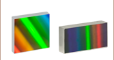
Click to Enlarge
Figure 1.1 Enlarged View of SAF795H Gain Chip on Submount with Heat Sink.
- Broad Tuning Range
- High Output Power
- Ultra-Low Angled Facet Reflectance: 0.005% (Typ.)
- Gain Medium for Narrow Linewidth Fiber Bragg Grating Lasers
- Gain Medium for Widely Tunable External Cavity Semiconductor Lasers
Single Angled Facet (SAF) gain chips use a geometric technique to further reduce the reflection on one end of the chip by curving the ridge waveguide so that it is not normally incident to the chip facet. This, in combination with an AR coating on that facet, virtually eliminates back reflections that can create unwanted feedback into the laser cavity. As a result, SAF gain chips are superior to standard gain chips when used in Extended Cavity Lasers (ECLs), particularly tunable ECLs, since any residual reflection from the AR-coated Fabry-Perot (FP) gain chip facet often limits the stability, output power, and spectral quality of the laser.
Thorlabs offers SAF gain chips with either low- or high-reflectivity coatings on the normal facet to support a wide range of external cavity configurations. For more information on the importance of normal facet reflectivity in these configurations, please see the ECL Tutorial tab. For sample results of SAF gain chips in external cavity laser setups suited to both low- and high-reflectivity coatings, please refer to the ECL Sample Results tab. Our SAF gain chips are available either on submounts alone or on submounts with a heatsink and cathode/anode leads attached.
Handling and Usage
These SAF gain chips are sensitive to electrostatic shock, they should always be handled using standard static avoidance practices.
These SAF gain chips are not intended to be used as Amplified Spontaneous Emission (ASE) sources as this will significantly decrease their lifetime. For more information on using the SAF gain chip in an external cavity laser, see the ECL Tutorial tab.
外部共振器型レーザ(ECL): 波長可変と狭帯域幅
レーザ動作に必要な2つの要素は(1)光信号を増幅する活性利得媒体と(2)レーザ発振を持続させるためのフィードバック(反射)機構です。ファブリペロー型レーザでは、Figure 41Aに示すように、r1とr2(それぞれのパワー反射率:R1 = r12とR2 = r22)の反射係数を持つ2枚のミラーによって、光電界がフィードバックされます。
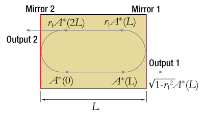
Figure 41A ファブリペロー型レーザの構造
長さLの共振器内における光電界の往復利得は、下記の数式で表現できます。
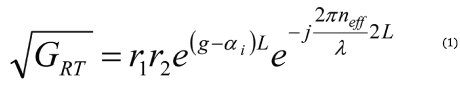
ここで、gは利得、αiは内部損失係数、λは真空中の波長、neffは有効屈折率、L は共振器長です。これより、最大振幅と位相条件は下記で表されます。
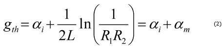

ここで、αmはミラーの損失、Nはモード数を表します。
半導体レーザでは、順方向にバイアス電圧を印加されたダイオードの接合領域に電流を注入することによって、利得媒体が励起されます。半導体レーザの量子井戸接合内に高濃度の電子と正孔が存在することによって、光利得に必要な反転分布状態を作ることができます。
利得媒体が半導体材料の場合、チップの端面におけるフレネル反射によってファブリペロー型共振器を構成することができます。接合領域は、実効的には両端面の間の導波路です。導波路に垂直な劈開しただけのコーティング無しの面は、反射率Rが約30%です。しかしながら、端面での反射率を光学コーティングで調整することによって、このデバイスの最大出力パワーを最適化することができます。ファブリペロー型半導体レーザの最大パワーは、後側端面に高反射率(HR)コーティング、前側端面に低反射率(LR)コーティングの場合で得られます。
ファブリペロー型半導体レーザーデバイスの発振スペクトルは、注入電流によって決まります。g > αi の閾値未満にバイアスされたとき、放射スペクトルでは、位相方程式によって定義されるファブリペロー型共振器の縦モードに相当するピークが広範囲に分布しています。注入電流が増加し、g = αi + αmに達するまでレーザ発振は起こりません。レーザ発振波長は、最初に閾値条件に達した縦モードによって決まります。出力スペクトルは、必ずしも1つのレーザ発振波長に収束するとは限らず、狭いスペクトル幅の複数の縦モードで構成されることがあります。
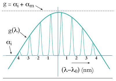
Figure 41B ファブリペロー型レーザの利得曲線
このことは、5~10 nmの光帯域幅を持つInPを用いたファブリペロー型レーザに特に当てはまります。GaAsを用いたデバイスでは、波長と出力パワーに依存して、単一縦モードで動作させることが可能です。典型的には出力波長帯域は2 nm未満です。
約300 μmの長さと約4の群屈折率を持つ典型的な850 nm半導体レーザは、長さが1 mmの1550 nm半導体レーザと同じく、0.3 nmの縦モード間隔を持っています。例えば、半導体レーザを加熱や冷却し、共振器の長さ、あるいは屈折率を変えることによって、全モードをシフトさせて、その結果、出力波長を変えることが可能です。
レーザ線幅
半導体レーザの単一縦モードの線幅(FWHM)は、線幅増大係数 αH [1]を含んだSchawlow-Townesの公式で与えられます。

ここで、hvは光子エネルギー、vgは群速度、nspは反転分布係数、Poutは一端面からの出力光強度です。この関係式は、コヒーレントレーザ発振モードに自然放出光が加わって生じる位相と振幅ゆらぎによるレーザ線幅のスペクトル空間広がりを表しています。いわゆる量子雑音ゆらぎは、レーザ線幅の下限を決定しますが、通常、機械的/音響振動的変動や熱変動によって生じる大きな雑音ゆらぎに埋もれます。
共振器長を大きくすると、相対的にαmが小さくなり(式(2)参照)、線幅が小さくなります。このことは、量子雑音限界の線幅の関係式(式(4)参照)を見ればわかります。共振器長を長くすることにより、自然放出光子数が減少(それぞれの縦モードの「cold-cavity」のスペクトル幅が減少)し、共振器内の全光子数が増加します。このため、Schalow-Townesの式に共振器長の関連項が2度現れます。
共振器長が0.3 mmの単一周波数分布帰還(DFB)型半導体レーザの典型的な発振線幅は、1~10 MHzオーダです。たとえば、共振器長を3 cmにすれば、発振線幅は100分の1以下になります。半導体レーザの共振器長をより長くして、発振線幅を1 kHz未満に減少させることができた例もあります[2] 。
単一波長の動作とチューニング
多くの用途では、発振波長または周波数、あるいはその両方が調整可能な単一縦モード(単一周波数)レーザが要望されています。これを実現するため、半導体レーザに外付けされた波長選択用フィードバック素子(共振器)を用いると発振波長を選択することができます。この外部共振器レーザ(ECL)を適切に動作させるには、外付けのフィードバックと干渉しないように、半導体チップのファブリペロー型共振器からの固有の戻り光の抑制が必要となります。利得チップのファブリペロー型共振器の影響は、チップの一方の端面にAR(反射防止)コーティングを行うことにより、減少させることができます。
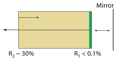
Figure 41C 利得チップを使った外部共振器の構造
少なくとも、チップの端面からの反射率(R1)は、外付けのフィードバック(ミラー)の反射率(R1)よりも20 dB以上小さくなければなりません。つまり、R1 < 10-2 x Rextです[3]。ARコーティングされた場合でも、ARコーティングされたファブリぺロー利得チップ端面からの反射により、特にレーザが波長可変の場合にECLの安定性、出力パワー、波長特性が制限されます。チップ端面での反射をより抑えるために、角度を付けた導波路とARコーティングの組み合わせによって、内部チップファブリペロー型共振器からのフィードバック(戻り光)の多くを取り除くことができます [4]。この片面角度付き(SAF)の利得チップにより、外部共振型レーザ(特に広帯域波長可変レーザ)はより優れた特性が得られます。
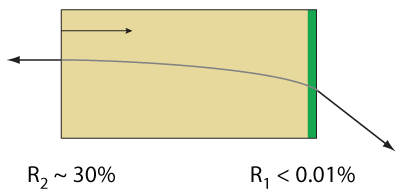
Figure 41D 片面角度付き利得チップ
外部共振器型レーザの設計
外部共振器型半導体レーザを実現するには様々なアプローチがあります [3]。いずれのアプローチにおいてもまず第1に考えなければならないのは、波長選択フィードバック素子を選ぶことです。最も一般的なフィードバック素子の1つである回折格子は、単一周波数および広範囲な可変外部共振器型レーザの両方にフィードバック素子として使用可能です。
利得チップからのコリメート光が、格子表面の垂線と角度θ、かつ回折ラインと垂直に回折格子に入射すると、回折ビームは以下の式で求められるθ'の角度で回折格子から出射します。
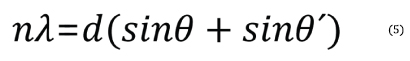
ここで、nは回折の次数、λは回折波長、dはグレーティング定数(溝間の距離)です。n > 0に対して、回折格子(グレーティング)は、波長に依存する角度θ'の角度で光を回折することにより、多くのスペクトルの入射光を空間的に分離します。利得チップからのスペクトル成分が空間的に分離されれば、特定波長の光を選択的に反射させて利得媒体内に戻すために様々な方法が利用できます。
外部共振型レーザ、リトロウ型構成
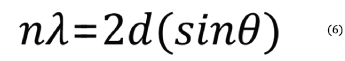
最も容易なアプローチの1つは、1次の回折光が利得チップに戻って再反射するように回折格子が配置されたリトロウ構成です(すなわち、上記の式(5)で、θ = θ')。
外部共振型レーザの構成に必要な光学素子(コリメート用レンズと回折格子)の数を最小にするために、回折格子の0次反射光からレーザ出力パワーを取り出すことができます。
回折格子を回転することによって、導波路に反射される光の波長が変わり、波長をチューニングすることができます。(一定の格子定数を持つ)回折格子、コリメートレンズ、共振器長を1つの縦モードだけが導波路の受光角内で利得チップに反射で戻ってくるように選択することで、外付け共振器レーザで単一周波数レーザースペクトルを得ることができます。半導体利得チップに戻す集光スポットサイズと、回折格子への照射スポットサイズに影響するコリメートレンズの選択は重要です。この構成の短所の1つは、波長をチューニングさせるときに0次オーダの出力ビームの角度が変化することです。しかしながら、外部共振器レーザの出力がSAF利得チップの垂直面からの出力光として得る場合、この問題を避けることができます。この構成では、SAF垂直面の典型的な反射率Rを約10%程度と小さくし、レーザの出力パワーを最大にするような次数の回折光が得られる回折格子を選択し外部共振器レーザを構成します。
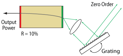
Figure 41E リトロウ型外部共振器レーザ
外部共振型レーザ、リットマン型構成
外部共振型レーザのもう1つの一般的な方式は、追加の調整ミラーを使ってフィードバック波長を選択するリットマン型構成です[5]。大きな入射角で回折グレーティングを2回通過する外部共振器は、よりよい波長選択性を持ちます。結果として、リットマン型の外部共振型レーザの光出力線は、リトロウの構成の場合に比べて狭い線幅になります。リットマン型の構成では、波長を変化させても伝搬方向は固定されたままなので、レーザ出力光は通常は回折格子の0次オーダの反射です。この場合、SAFの直角面は、ECL内部の損失を最小にして出力パワーを最大にし、出力強度を最大にするために典型的には90%以上の高反射率(HR)でコーティングされます。
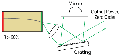
Figure 41F リットマン型外部共振器レーザ
用途によっては、レーザの出力部として、SAF利得チップの垂直面の利用が望ましいこともあります。この用途に対しては、SAF利得チップの垂直面上のコーティングは、レーザの出力強度を最大にするために低反射率とする必要があります。
リットマン型の弱点は、共振器の内部損失がリトロウの構成の場合より高く、したがって、レーザの出力強度が一般的には低いことです。内部損失が大きくなるのは、主に可変ミラーからのゼロオーダ反射光の損失および大きな入射角で光を反射させたとき、回折格子の効率が下がることです。
外部共振器型レーザの設計について
SAF利得チップでは、外部共振器内の利得チップの端面からの望ましくない反射光によるフィードバックを除去されるため、外部共振器型レーザの使用に適しています。当社では、様々な外部共振器の構成を可能にするために、垂直面上に低反射率または高反射率コーティングの両方のSAFチップ をご提供しています。特に外部共振器型レーザ構成の性能を最適化するための特注コーティングに関しては、当社までお問い合わせください。
参考文献
(1) Henry, C. H., "Theory of the Linewidth of Semiconductor Lasers." IEEE J. of Quantum Electron QE-18, 259 (1982).
(2) Wyatt, R., Cameron, K. H., and Matthews, M. R. "Tunable Narrow Line External Cavity Lasers for Coherent Optical Communication Systems." Br. Telecom. Technol. J. 3, 5 (1985).
(3) Zorabedian, P. "Tunable External Cavity Semiconductor Lasers." Tunable Lasers Handbook Ed. Duarte, F. J. New York, Academic, 1995. Chapter 8.
(4) Heim, P. J. S., Fan, Z. F., Cho, S.-H., Nam, K., Dagenais, M., Johnson, F. G., and Leavitt, R. "Single-angled-facet Laser Diode for Widely Tunable External Cavity Semiconductor Lasers with High Spectral Purity." Electron. Lett. 33, 1387 (1997).
(5) Littman, M. G. and Metcalf, H. J. "Spectrally narrow pulsed dye laser without beam expander." Appl. Opt. 17, 2224 (1978).
Sample Results of an SAF1093C Used in a Basic Littrow Configuration
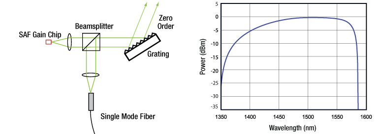
Figure 3.1 Sample power spectrum generated by an SAF1093C gain chip in an external cavity laser. A Littrow configuration, as shown in the diagram, was used for the external cavity design due to the SAF1093C’s high normal facet reflectivity of 90%. For more information on this configuration and the use of gain chips in external cavity lasers, please refer to the ECL Tutorial tab.
Sample Results of an SAF1144C Used in a Basic Littman-Metcalf Configuration
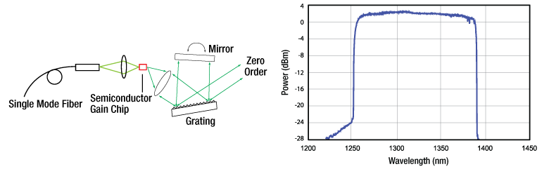
Figure 3.2 Sample power spectrum generated by an SAF1144C gain chip in an external cavity laser. A Littman-Metcalf configuration, as shown in the diagram, was used for the external cavity design due to the SAF1144C's low normal facet reflectivity of 10%. For more information on this configuration and the use of gain chips in external cavity lasers, please refer to the ECL Tutorial tab.
Click to Enlarge
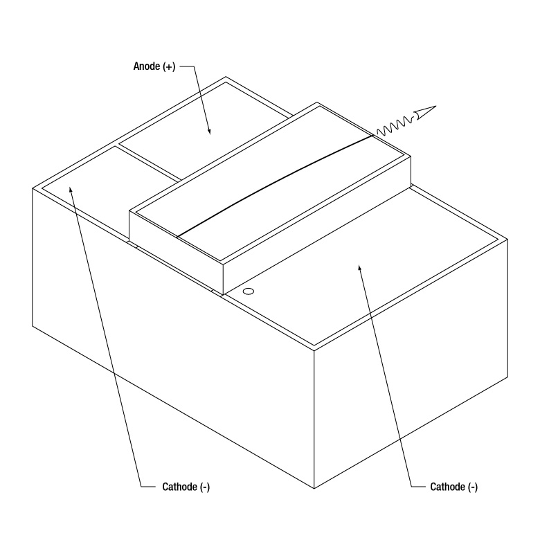
Figure 4.1 Diagram of the anode and cathode pins of SAF gain chip on submount. Please note that dimensions of chip vary depending on item #.

Click to Enlarge
Figure 4.2 Diagram of the anode and cathode Pins of SAF gain chip on submount with heat sink. Please note that dimensions of chip vary depending on item #.
| Posted Comments: | |
| No Comments Posted |
Click the ![]() icon below for more detailed performance specifications.
icon below for more detailed performance specifications.
| Table G1.1 Key Specificationsa,b | |||||||
|---|---|---|---|---|---|---|---|
| Item # | Info | ASE Center Wavelength | Optical Bandwidthc,d | ASE Powerd | Normal Facet Reflectivity | Lateral Beam Exit Angle | Operating Current (Typ./Max) |
| SAF795C | 800 nm | 12 nm | 55 mW | 90% | 19.5° | 250 mA/300 mA | |
| SAF815C | 815 nm | 13 nm | 50 mW | 90% | 19.5° | 250 mA/300 mA | |
| SAF852C | 853 nm | 10 nm | 95 mW | 90% | 19.5° | 250 mA/300 mA | |
| SAF1064C | 1080 nm | 25 nm | 120 mW | 90% | 19.5° | 400 mA/450 mA | |
| SAF1145C | 1220 nm | 80 nm | 1.0 mW | 10% | 26.5° | 300 mA/500 mA | |
| SAF1144C | 1320 nm | 50 nm | 20 mW | 10% | 26.5° | 600 mA/800 mA | |
| SAF1093C | 1450 nm | 95 nm | 20 mW | 90% | 26.5° | 500 mA/800 mA | |
| SAF1126Ce | 1517 nm | 75 nm | 0.5 mW | 10% | 19.5° | 300 mA/350 mA | |
| SAF1118Ce | 1573 nm | 79 nm | 1.7 mW | 10% | 19.5° | 300 mA/350 mA | |
| SAF1091C | 1650 nm | 90 nm | 1.3 mW | 90% | 26.5° | 500 mA/800 mA | |
- Specifications are given at a chip temperature TChip = 25 °C. All quoted values are typical, unless otherwise indicated.
- These Single Active Facet (SAF) gain chips are meant to be used in external cavity lasers. Product lifetime will be significantly reduced by using it in an Amplified Spontaneous Emission mode.
- Specified as the Width of the ASE Spectrum 3 dB Below the Peak
- Specified at Operating Current (Typ.)
- Specifications for gain chip in a Littrow external cavity configuration available by clicking the
 icon.
icon.
Click the ![]() icon for more detailed performance specifications.
icon for more detailed performance specifications.
| Table G2.1 Key Specificationsa,b | |||||||
|---|---|---|---|---|---|---|---|
| Item # | Info | ASE Center Wavelength | Optical Bandwidthc,d | ASE Powerd | Normal Facet Reflectivity | Lateral Beam Exit Angle | Operating Current (Typ./Max) |
| SAF795H | 800 nm | 12 nm | 55 mW | 90% | 19.5° | 250 mA/300 mA | |
| SAF815H | 815 nm | 13 nm | 50 mW | 90% | 19.5° | 250 mA/300 mA | |
| SAF852H | 853 nm | 10 nm | 95 mW | 90% | 19.5° | 250 mA/300 mA | |
| SAF1064H | 1080 nm | 25 nm | 120 mW | 90% | 19.5° | 400 mA/450 mA | |
| SAF1145H | 1220 nm | 80 nm | 1.0 mW | 10% | 26.5° | 300 mA/500 mA | |
| SAF1144H | 1320 nm | 50 nm | 20 mW | 10% | 26.5° | 600 mA/800 mA | |
| SAF1093H | 1450 nm | 95 nm | 20 mW | 90% | 26.5° | 500 mA/800 mA | |
| SAF1126He | 1517 nm | 75 nm | 0.5 mW | 10% | 19.5° | 300 mA/350 mA | |
| SAF1118He | 1573 nm | 79 nm | 1.7 mW | 10% | 19.5° | 300 mA/350 mA | |
| SAF1091H | 1650 nm | 90 nm | 1.3 mW | 90% | 19.5° | 500 mA/800 mA | |
- Specifications are given at a chip temperature TChip = 25 °C. All quoted values are typical, unless otherwise indicated.
- These Single Active Facet (SAF) gain chips are meant to be used in external cavity lasers. Product lifetime will be significantly reduced by using it in an Amplified Spontaneous Emission mode.
- Specified as the Width of the ASE Spectrum 3 dB Below the Peak
- Specified at Operating Current (Typ.)
- Specifications for gain chip in a Littrow external cavity configuration available by clicking the icon.