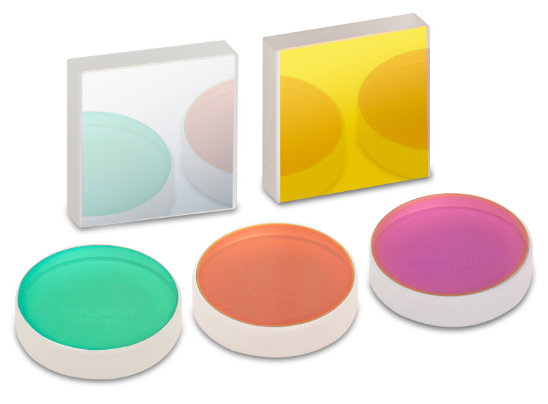
 Products Home
光学コーティング
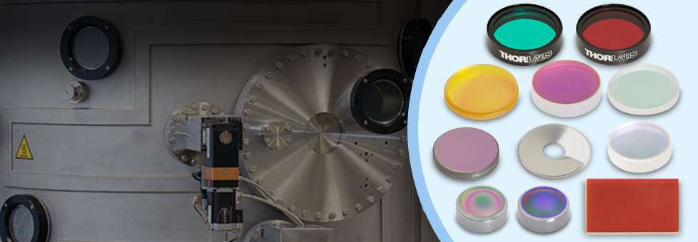
- State-of-the-Art, In-House Coating Lab
- Broad Range of Coating Capabilites on a Wide Variety of Substrates

Please Wait

当社におけるコーティング工程
当社では最新技術を有する光学コーティング部門を社内にもつことで、金属コーティングから反射防止コーティング、そして最先端のイオンビームスパッタ(IBS)コーティングからプラズマコーティングに至るまでを自社内からご提供しております。この大型設備は、標準品の光学素子を社内で大量生産するだけではなく、お客様の多様なニーズに合ったカスタム仕様の光学素子製造の可能性の拡大にも利用されています。
コーティングの設計
Click to Enlarge
積層コーティング
スペクトル性能をはじめとした光学薄膜の主な特長は、コーティング層の構造と数、使用材質の屈折率、そして光学素子の材質の光学特性で決まります。
ほとんどのコーティングは、明瞭な境界を持つ高い屈折率と低い屈折率の材質層が交互に重なった構造となっています。積層構造の相違が、コーティング特性の違いとなります(バンドパス、エッジパス、BBARなど)。規定の波長範囲における性能を最適化するために、層の厚さや反射率が精密に制御されています。当社では豊富な薄膜モデリングツールがあるので、特定のコーティング性能の様々な側面に着目した設計、評価や最適化が実現できます。
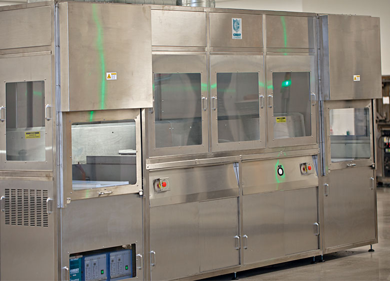
クリーニング
光学素子のコーティング工程における最初で最も重要な工程の1つは、自動化された超音波洗浄ラインで行われる、コーティング前の基板のクリーニングです。溶剤や洗浄剤を用いた超音波槽を複数使って、光学素子の基板表面に付着した異なる種類の汚れを各槽で順次除去します。この工程によって、表面の汚れがコーティングの基板に対する接着性を妨げることを防止します。
Click to Enlarge
完全自動化された光学部品クリーニングシステム

Click to Enlarge
クリーニング後の光学素子
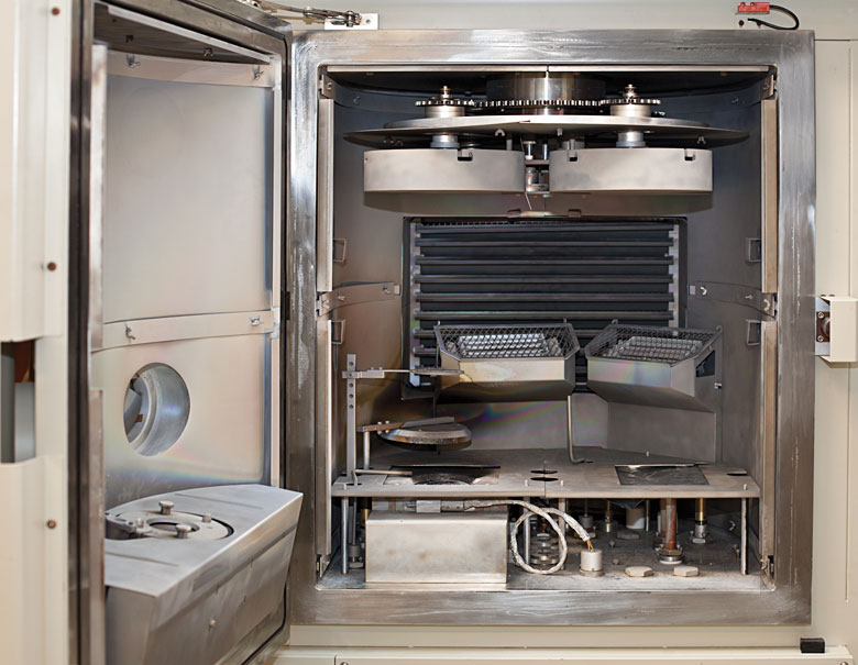
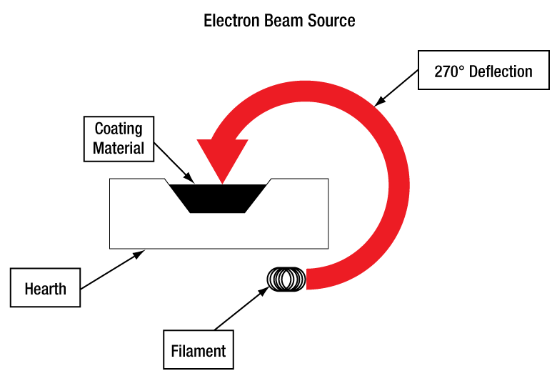
電子ビーム蒸着
現在、当社のコーティング設備では、4つの完全自動化電子ビーム(E-ビーム)蒸着システムが稼働しています。これらのシステムでは電子ビーム銃を利用して遷移金属酸化物(TiO2、Ta2O5、HfO2、Nb2O5、ZrO2)、金属ハロゲン化物(MgF2、YF3)またはSiO2などを蒸発させます。このようなプロセスは、基板への良好な接着性や最終的なコーティングにおいて要求される材質特性を得るために、高い温度(200~250°C)で行われる必要があります。
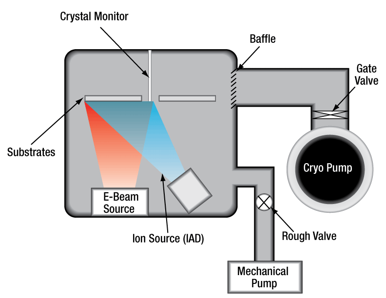
イオンビームアシスト蒸着
イオンビームアシスト蒸着(IAD)では、電子ビーム蒸着と同様にコーティング材を蒸発させますが、さらにイオン銃を用いて低温(20~100°C)で核形成と材料の成長を促進します。イオン銃を利用することで、温度に敏感な基板もコーティング可能になります。この工程では高濃度のコーティングになるので、周囲環境の湿気や乾燥によるスペクトルシフトを抑制することができます。

IBS蒸着
当社のイオンビームスパッタリング(IBS)蒸着チャンバは、コーティング設備の中でも最新の装置です。この技術では、高いエネルギ値の高周波プラズマ銃を使って、コーティング材をスパッタリングすることで基板に蒸着させる一方で、別のRFイオン銃(アシスト用)が蒸着工程中にIAD機能を実現します。スパッタリングとは、イオン銃が放出するイオン化したガス分子がターゲット材料の原子に衝突する運動エネルギを利用した工程です。この現象は、ビリヤードでキューボールが最初にオブジェクトボールを散らすブレイクショットと似ており、この現象が分子レベルで周りに他のボールもある状態で行われている様子と似ています。
IBSの利点
- 工程管理が容易
- 幅広いコーティング設計が可能
- 優れた表面品質と散乱の最小化
- スペクトルシフトを低減
- 1回の製造サイクルで厚みのあるコーティング
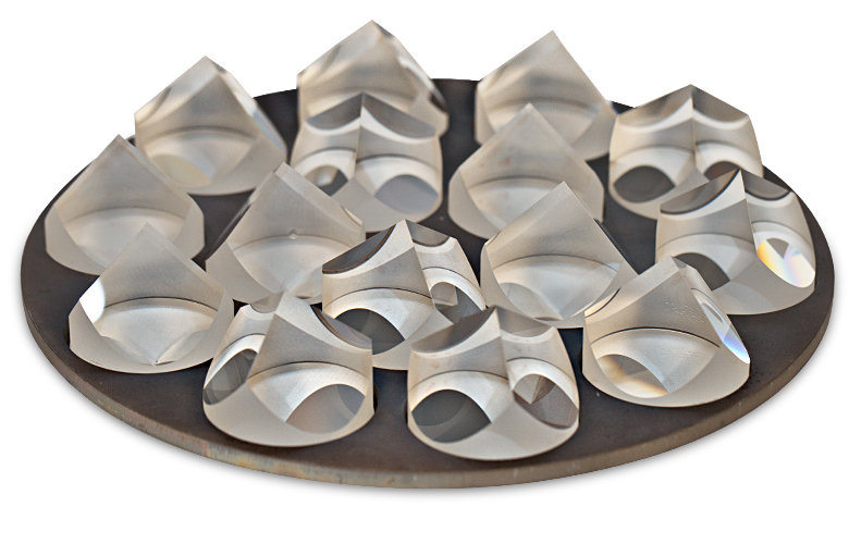
Click to Enlarge
コーティング付きレトロリフレクタ
計測
当社では、研究用途クラスの吸光分光法の装置を用いて、UV域から遠赤外線域までの波長での性能評価を行っています。 Varian Cary 5000やPE Lambda 950の分光光度計は、UV域~可視域~近赤外域までのコーティングのスペクトル特性評価に用いられ、Olis PE 983の赤外域分光光度計が赤外域(2~55.5 µm)対応のコーティングに用いられています。吸光分光法の装置の他にも、ご提供する光学素子を試験・評価するために、さまざまなレーザや半導体レーザ光源、当社のパワーメータやディテクタ、偏光計の製品シリーズを使っています。標準品、特注品、組み込み用途(OEM用途)向け製品など、当社が提供するすべての光学素子が仕様範囲で正常に機能することを確認するために、独自の計測装置のセットアップも構築しています。なお当社の計測装置は全て、ISO9001:2015規格に準じて定期的に校正されています。
レーザーラインフィルタとバンドパスフィルタ
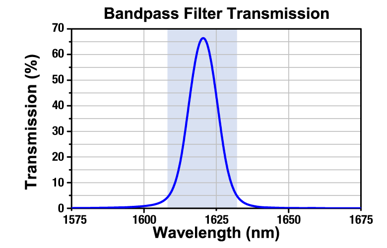
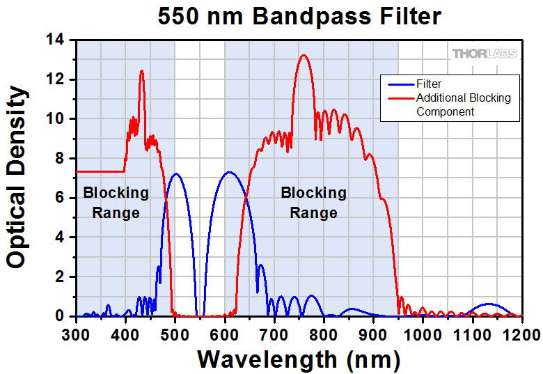
レーザーラインフィルタとバンドパスフィルタは、不要なスペクトル域の光を阻止し、規定の狭いスペクトル領域だけを透過するフィルタです。この種のフィルタは、まず規定のバンドパス領域で高い透過性を示し、その両側の帯域ではある程度の波長領域までの光をブロックします。この特性の不足した部分を補うために、要求仕様に合わせて誘電体か金属誘電体による光をブロックするコーティングを追加します。阻止帯域を広げるため、その(阻止)帯域のさらに外側まで光をブロックする光学素子を追加しています。しかし、透過帯域における透過率は若干低下しています。
このコーティングでは、真空蒸着コーティング技術を用いて、偶数次数のスペーサ層で分離される2つの反射層のスタックが形成されます。このような反射積層は、高低2種の屈折率からなる物質で構成され、反射率は99.99%を超えることがあります。スペーサ層の厚みおよび反射層の数の両方または片方を変えることで、フィルタの中心波長および帯域を変更することができます。
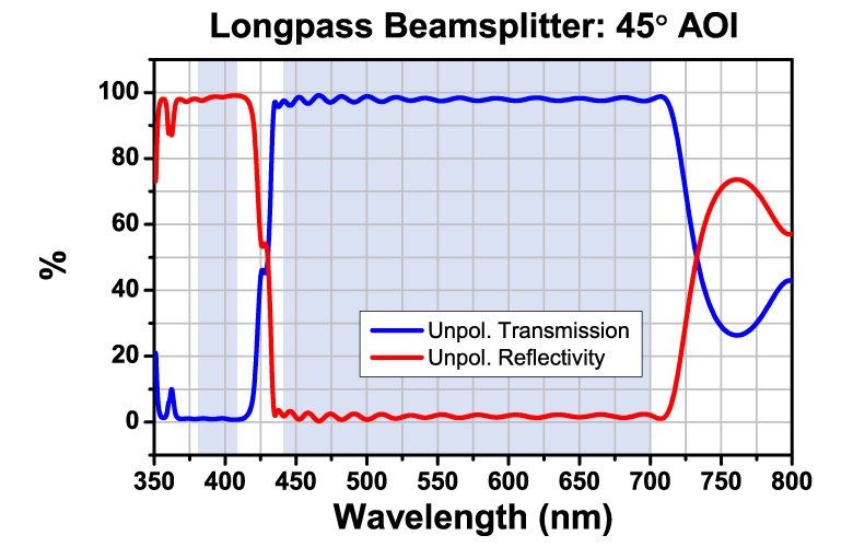
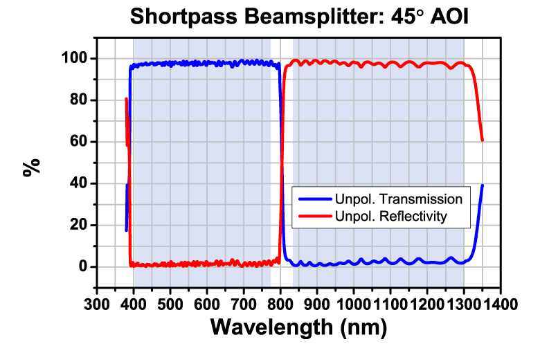
エッジパスフィルタ
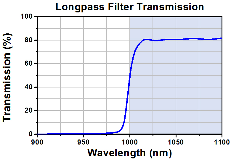
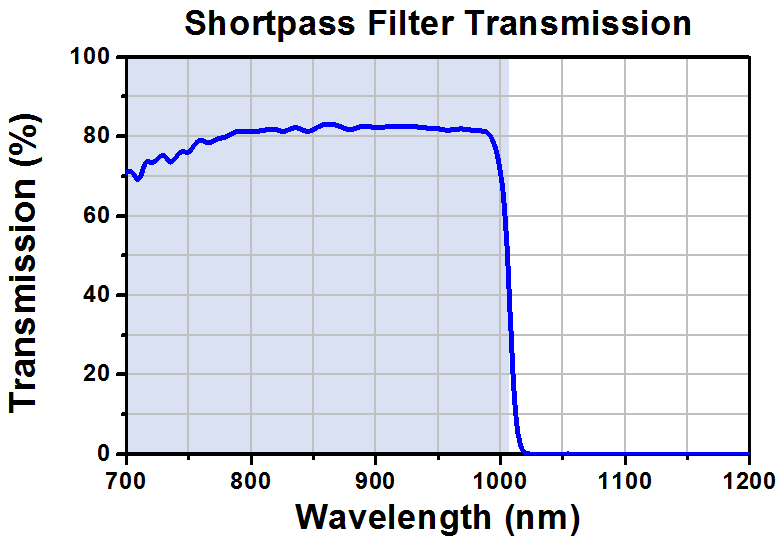
エッジパスフィルタは、特定の波長範囲を分離するのに便利です。ロングパスフィルタは、カットオフ波長よりも長い波長の光を透過し、カットオフ波長よりも短い波長の光を阻止します。ショートパスフィルタは、カットオフ波長よりも長い波長を阻止し、カットオフ波長よりも短い波長を透過します。
当社の全てのエッジパスフィルタには、耐久性のある誘電体コーティングが施されているので、通常行うクリーニングや取扱では、表面に傷がつきにくくなっています。薄膜層の構造は、基本的に1/4波長層を積層したもので、スペクトルの分離には吸収ではなく干渉効果を利用しています。
ダイクロイックビームスプリッタ
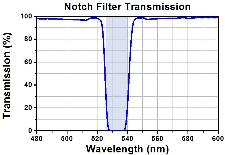
ノッチフィルタ
 Click to Enlarge
ノッチフィルタは、一般的にバンドストップフィルタまたは帯域防止フィルタとも呼ばれていますが、特定の波長帯域(ストップバンド)の光を非常に低いレベルに減衰させて、それ以外の波長の光を透過します。その機能はバンドパスフィルタの逆で、同じ方法で製造されています。
ND(減光)フィルタ
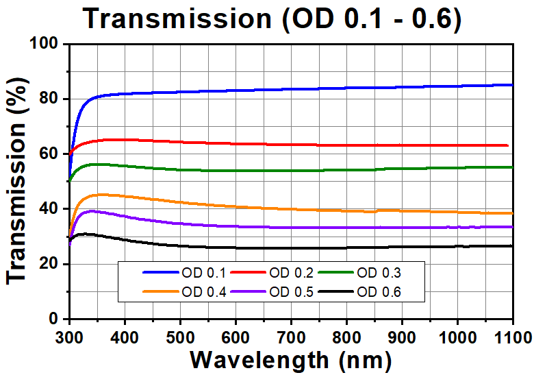
NDフィルタは、所定の範囲の全ての波長を一定の割合で減衰させ、検知装置の損傷防止に用いられます。固定式NDフィルタでは、減衰される光量は一定です。一方で可変式NDフィルタ表面のフィルムは、一定の面積ごとに膜厚が段階的に変化していく構造となっており、用途によって減衰光量を変化させることができます。連続型可変式NDフィルタでは、フィルタ上で連続的に膜厚が変化します。つまり減衰量を連続的に変化させることができます。当社のご提供する連続型可変式NDフィルタには、長方形タイプと円形タイプがあります。
反射防止(AR)コーティングは、硬く、耐熱性の高い酸化膜コーティングで、光学素子の表面に成膜されると、規定の波長範囲における光の表面反射を最小限に抑えます。ARコーティングが成膜されていない場合は、反射によって光学表面で4%程度の光が失われます。例えば、コーティング無しのレンズが3枚続けて使われている場合、6つの面において入射光がそれぞれ4%ずつ失われることになります。従って、合計で21.7%の光の損失となります。上記の例で、Bコーティング(一面あたりRavg<0.5%)付きのARコーティングレンズを使うと、表面反射によって失われる光の総量は3%以下になります。従って、ARコーティング付きの光学素子を使うことで、透過率が78.3%から97%以上に改善されることになります。なお、コーティング無しの光学素子の光損失量を4%としていますが、この数値は概算値であり、材質や入射角(AOI)によって大きく変わる点にご注意ください。
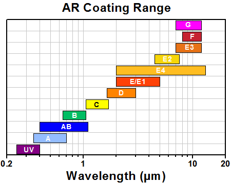
下のグラフは、当社の各ARコーティングの波長範囲を示しています。グラフ内の各ARコーティングのカラーバーをクリックするとそれぞれの性能プロットをご覧いただけます。
広帯域反射防止(BBAR)コーティングは、反射率の高い材質と低い材質を交互に重ねた多層のコーティングです。コーティング層は、基板に電子ビーム蒸着で形成されます。各層の厚さは、各層からの反射光の波同士は干渉により打ち消し合い、透過光の波は干渉により強め合うように、モデリングソフトウェアで最適化します。その結果、光学素子は特定の波長域で優れた透過性能を有し、内部反射(ゴースト現象)も最小限に抑制されます。当社のBBARコーティングは、0°~30°の入射角、0.5の開口数(NA)で性能を発揮します。現在当社では、8種類の波長範囲に対応したBBARコーティングをご用意しています。
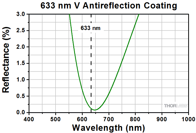
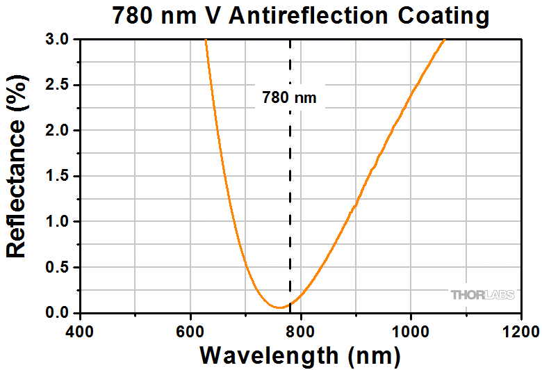
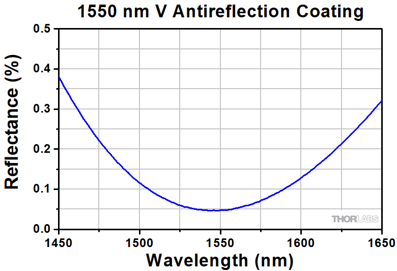
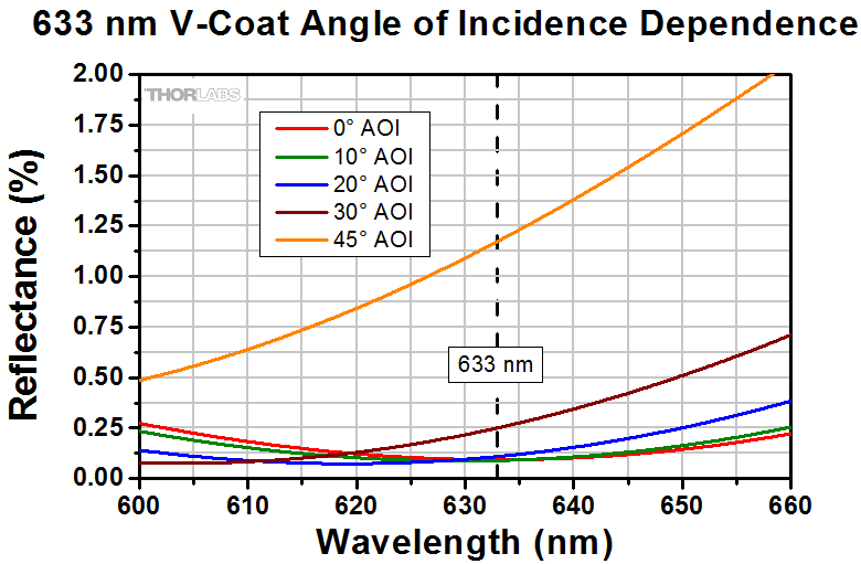
Vコーティングは、誘電体多層反射防止薄膜で、狭い波長範囲で反射率を最小化するように設計されています。表面反射率はこの最小反射率の波長の両側で急速に大きくなり、反射率曲線は「V字型」を描きます。広帯域ARコーティングと比較すると、Vコーティングでは、設計入射角の範囲で使用するかぎり、その狭い波長域ではより小さな反射率が得られます。右のグラフは、0°の入射角用に設計された633 nm Vコーティングの様々な入射角に対する反射率の例です。当社では様々な種類のVコーティングをご用意しております。詳細は下の表をご覧ください。
下の表では、当社の多くの光学素子製品に施されているARコーティングの仕様をご紹介しています。なお、当社では外部ベンダによってコーティングされた光学素子もご提供しております。従って当社のARコーティング付き光学素子の仕様は、このページの内容と若干異なる場合もあります。個々の製品のARコーティングの仕様は、各製品ページに必ず記載されているのでご参照ください。
| Broadband Antireflective Coating Specifications | ||||
|---|---|---|---|---|
| Coating Code | Wavelength Range | Reflectancea | Performance Plotb | Coating Variationc |
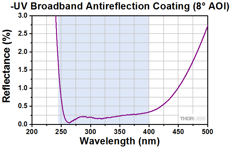
| UV | 245 - 400 nmd | Ravg < 0.5% | Unavailable | |
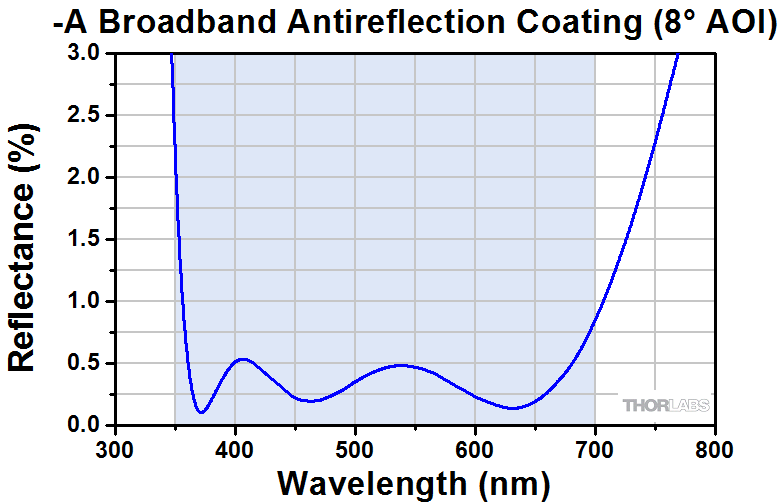
| A | 350 - 700 nm | Ravg < 0.5% | 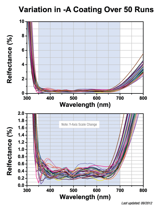 Raw Data | |
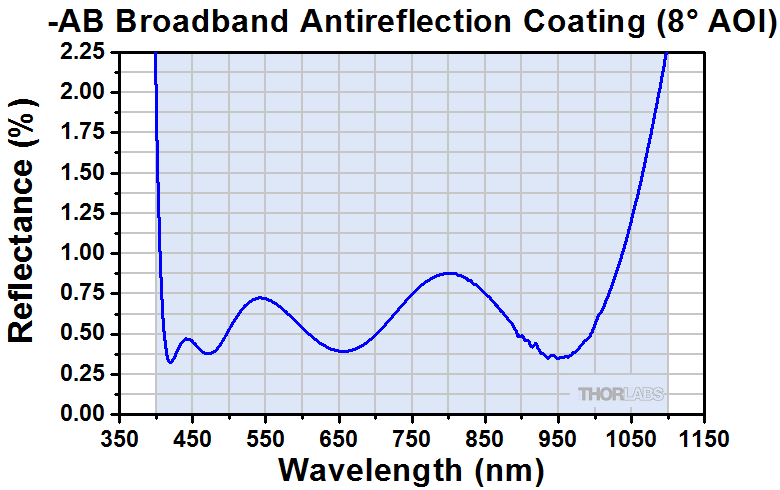
| AB | 400 - 1100 nm | Ravg < 1.0% | Unavailable | |
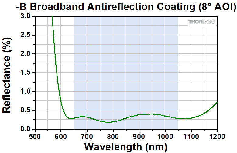
| B | 650 - 1050 nm | Ravg < 0.5% | 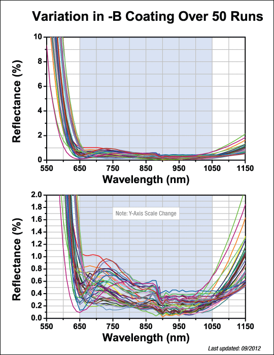 Raw Data | |
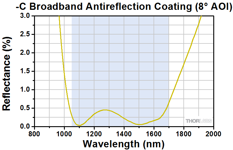
| C | 1050 - 1700 nme | Ravg < 0.5% |  Raw Data | |
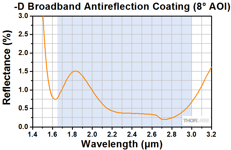
| D | 1.65 - 3.0 µm | Ravg < 1.0% | Unavailable | |
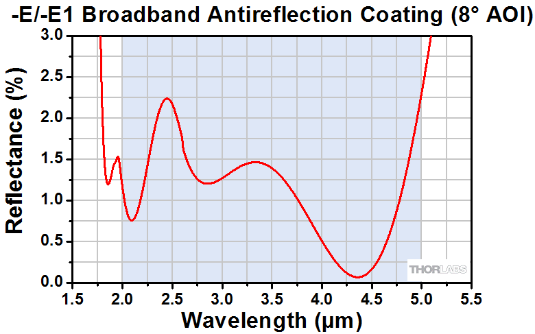
| Ef,g | 2 - 5 µm | Ravg < 1.25% | Unavailable | |
| E1g | 2 - 5 µm | Ravg < 1.50% Rabs < 3.0% | ||
| E4 | 2 - 13 µm | Ravg < 3.5% Rabs < 6% | 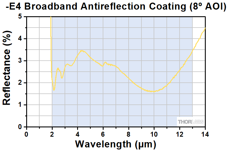 Raw Data | Unavailable |
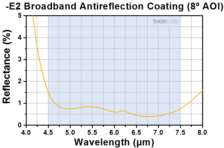
| E2 | 4.5 - 7.5 µm | Ravg < 1.0% Rabs < 2.0% | Unavailable | |
| E3h | 7 - 12 µm | Ravg < 1.0% Rabs < 2.0% | Unavailable | |
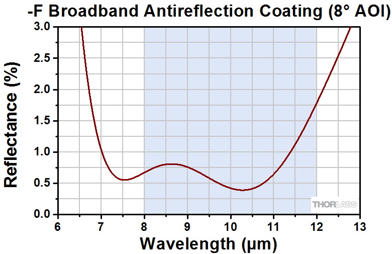
| F | 8 - 12 µm | Ravg < 1.5% | Unavailable | |
| Gh | 7 - 12 µm | Ravg < 1.0% | Unavailable | |
| Narrowband Antireflective (V-) Coating Specifications | |||
|---|---|---|---|
| Coating Code | Design Wavelength | Reflectance per Surfacea | Performance Plot |
| 405 | 405 nm | < 0.25% | 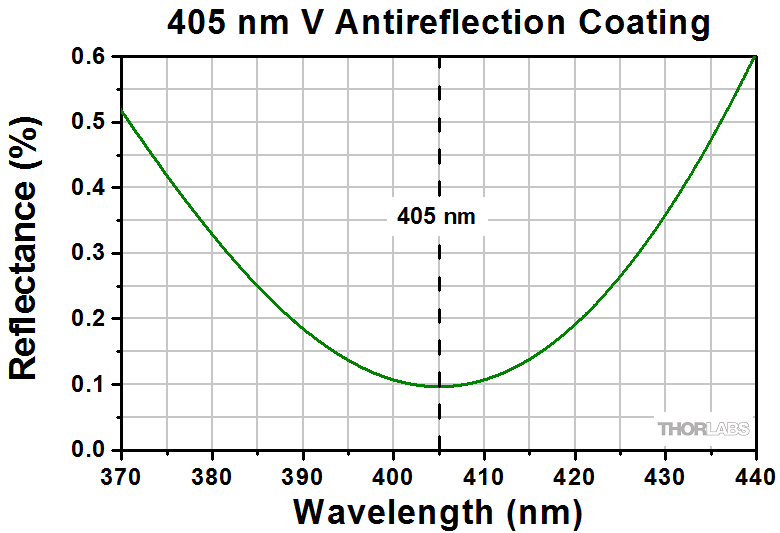 Raw Data |
| 532 | 532 nm | < 0.25% | 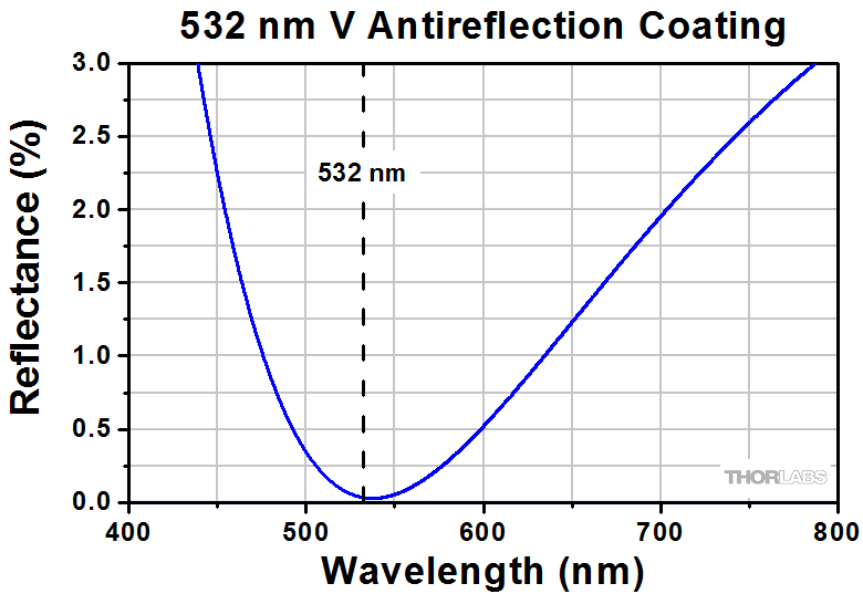 Raw Data |
| 633 | 633 nm | < 0.25% | |
| 780 | 780 nm | < 0.25% | |
| 1064 | 1064 nm | < 0.25% | 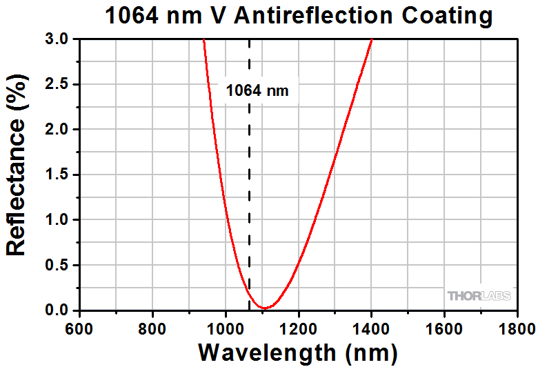 Raw Data |
| YAG | 532/1064 nm | < 0.25% | |
| 1550 | 1550 nm | < 0.25% | |

Click to Enlarge
入射角0°用633 nm Vコーティングの反射特性の入射角依存性
 当社でご提供しているHRコーティング付き光学素子
目次
当社では誘電体および金属による広帯域コーティング、レーザーライン用の誘電体狭帯域コーティング、ならびに高性能の結晶ミラーコーティングをご用意しています。 また、フェムト秒パルスレーザのための超短パルス光用ミラーもございます。
誘電体HRコーティングには広帯域用と狭帯域用がございます。いずれも硬質で耐熱性のある酸化皮膜で、仕様に示す波長範囲や入射角で表面反射率が最大となるように設計されています。このコーティングは、屈折率の低い物質と高い物質が交互に重ねられた層構造になっています。各層の厚さは、反射光の波は強め合うように干渉し、透過光の波は弱め合うように干渉するよう、モデリングソフトウェアで最適化されています。
HRコーティングを施すことで、表面の反射率は大きく向上しますが、その特性は波長と入射角(AOI)の両方に依存します。入射角が大きいと、特性は入射光の偏光にも依存します。HRコーティングの反射率についての詳細は下の表でご覧いただけます。
広帯域HRコーティング
当社では様々な性能パラメータに最適化された広帯域HRコーティングをご提供しています。下の図は、当社の広帯域HRコーティングの波長範囲の仕様を示しています。この図の該当するコーティングのバーをクリックすると、各コーティングの特性がグラフ表示されます。こちらをクリックしていただくと、当社の全ての広帯域HRコーティングを比較する生データをご覧いただけます。
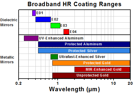
E01、E02、E03およびE04の誘電体HRコーティングは、広い波長域で高い反射率を有します。当社のUV域強化アルミニウムコーティングは、UV域の平均反射率を向上させるためにMgF2でオーバーコーティングされています。保護膜付きアルミニウムコーティングは低価格ですが、研究や工業用として使いやすいようにSiO2でオーバーコーティングされています。保護膜付き銀コーティングは可視(VIS)域で最も高い反射率を有し、また酸化防止のために表面はSiO2でオーバーコーティングされています。超短パルス光用銀コーティングは、小さな群遅延分散が得られるように形成されています。金コーティングは、保護膜付き、中赤外(MIR)域反射強化型、保護膜無しの3種類をご用意しております。保護膜付き金コーティングは800 nmまで高い反射率を維持します。中赤外域反射強化型金コーティングは、一般的な金ミラーにみられる中赤外域での損失を低減するように最適化されています。これらの金コーティングには保護用のオーバーコーティングが施されており、それによりミラーのクリーニングも容易になっています。保護膜無しの金コーティングは、保護膜付きの金コーティングに比べて高い反射率を有する一方で、やや損傷しやすいという特徴があります。
| Broadband HR Coating Specifications | ||||||||
|---|---|---|---|---|---|---|---|---|
| Coating Namea | Wavelength Range | Avg. Reflectanceb | Angle of Incidence | Graphs | Pulsed Laser Damage Threshold for UV Fused Silicac | CW Laser Damage Threshold for UV Fused Silicad | ||
| E01 | 350 - 400 nm | >99% | 0° to 45° | 1 J/cm2 (355 nm, 10 ns, 10 Hz, Ø0.373 mm) | - | |||
| E02 | 400 - 750 nm | >99% | 0° to 45° | 0.25 J/cm2 (532 nm, 10 ns, 10 Hz, Ø0.803 mm) | 550 W/cm (532 nm, Ø1.000 mm) | |||
| E03 | 750 - 1100 nm | >99% | 0° to 45° | 0.205 J/cm2 (800 nm, 99 fs, 1 kHz, Ø0.166 mm) 1 J/cm2 (810 nm, 10 ns, 10 Hz, Ø0.133 mm) 0.5 J/cm2 (1064 nm, 10 ns, 10 Hz, Ø0.433 mm) | 10 kW/cm (1070 nm, Ø0.971 mm) | |||
| E04 | 1280 - 1600 nm | >99% | 0° to 45° | 2.5 J/cm2 (1542 nm, 10 ns, 10 Hz, Ø0.181 mm) | 350 W/cm (1540 nm, Ø1.030 mm) | |||
| UV-Enhanced Aluminum (-F01) | 250 - 450 nm | >90% | 0° to 45° | 0.25 J/cm2 (266 nm, 10 ns, 10 Hz, Ø0.150 mm) 0.3 J/cm2 (355 nm, 10 ns, 10 Hz, Ø0.381 mm) | 300 W/cm (1.064 µm, Ø0.044 mm) 500 W/cm (10.6 µm, Ø0.339 mm) | |||
| Protected Aluminum (-G01) | 450 nm - 20 µm | >90% (450 nm - 2 µm) >95% (2 - 20 µm) | 0° to 45° | 0.3 J/cm2 (1064 nm, 10 ns, 10 Hz, Ø1.000 mm) | 100 W/cm (1.070 µm, Ø0.098 mm) 350 W/cm (10.6 µm, Ø0.339 mm) | |||
| Ultrafast-Enhanced Silver (-AG) | 750 nm - 1 µm | Rabsolute,S > 99.0% Rabsolute,P > 98.5% | 45° | 0.18 J/cm2 (800 nm, 52 fs FWHM S-Pol, 1000 Pulses)e 0.39 J/cm2 (800 nm, 52 fs FWHM S-Pol, Single Pulse)e | - | |||
| Protected Silver (-P01) | 450 nm - 20 µm | >96.5% (450 nm - 2 µm)f,g >95% (2 - 20 µm) | 0° to 45° | 0.225 J/cm2 (800 nm, 99 fs, 1 kHz, Ø0.167 mm) 1 J/cm2 (1064 nm, 10 ns, 10 Hz, Ø1.010 mm) | 500 W/cm (1.07 µm, Ø0.974 mm) 1500 W/cm (10.6 µm, Ø0.339 mm) | |||
| Protected Silver (-P02)h | 450 nm - 20 µm | >97% (450 nm - 2 µm) >95% (2 - 20 µm) | 0° to 45° | - | - | |||
| Protected Gold (-M01) | 800 nm - 20 µm | >96% | 0° to 45° | 2 J/cm2 (1064 nm, 10 ns, 10 Hz, Ø1.000 mm) | 500 W/cm (1.070 µm, Ø0.089 mm) 750 W/cm (10.6 µm, Ø0.339 mm) | |||
| MIR Enhanced Gold (-M02) | 2 - 20 µm | >98% | 0° to 45° | 0.1 J/cm2 (1.064 µm, 10 ns, 10 Hz, Ø1.06 mm) 3 J/cm2 (10.6 µm, 100 ns, 1 Hz, Ø1.29 mm) | 25 W/cm (1.07 µm, Ø1.04 mm) 450 W/cm (10.6 µm, Ø1.18 mm) | |||
| Unprotected Gold (-M03) | 800 nm - 20 µm | >97% | 0° to 45° | 4 J/cm2 (10.6 µm, 100 ns, 1 Hz, Ø0.435 mm) | 1000 W/cm (10.6 µm, Ø1.18 mm) | |||
狭帯域レーザーライン用HRコーティング
様々な性能パラメータに最適化されたHRコーティングをご提供しています。こちらの誘電体HRコーティングは、仕様のレーザーライン波長範囲で非常に高い反射率を有します。
| Narrowband Laser Line HR Coating Specifications | |||||||
|---|---|---|---|---|---|---|---|
| Coating Namea | Wavelength Range | Laser Line | Average Reflectanceb | Angle of Incidence | Graphs | Pulsed Laser Damage Thresholdc | CW Laser Damage Thresholdd |
| K04 | 262 - 266 nm | Nd:YAG, 4th Harmonic | > 99.0% (S- and P-Pol) | 0° to 45° | 2 J/cm2 (266 nm, 10 ns, 10 Hz, Ø0.416 mm) | - | |
| K05 | 300 - 308 nm | Ar Ion | > 99.5% (S-Pol) > 98.0% (P-Pol) | 0° to 45° | - | - | |
| K07 | 333 - 364 nm | Ar Ion | > 99.5% (S-Pol, 45° AOI)e > 99.0% (P-Pol, 45° AOI)e > 98.7% (Unpol, 0° AOI)e | 0° to 45° | 5 J/cm2 (355 nm, 10 ns, 10 Hz, Ø0.294 mm) | - | |
| K08 | 349 - 355 nm | Nd:YAG, 3rd Harmonic | > 99.5% (S- and P-Pol) | 0° to 45° | 3.5 J/cm2 (355 nm, 10 ns, 10 Hz, Ø0.350 mm) | - | |
| K10 | 458 - 528 nm | Ar Ion | > 99.0% (S- and P-Pol) | 0° to 45° | - | - | |
| J11 | 520 - 647 nm | Kr Ion | > 99.7% (S- and P-Pol) | 45° | - | - | |
| K12 | 524 - 532 nm | Nd:YAG, 2nd Harmonic | > 99.5% (S-Pol) > 99.0% (P-Pol) | 0° to 45° | 8 J/cm2 (532 nm, 10 ns, 10 Hz, Ø0.491 mm) | 550 W/cm (532 nm, Ø1.000 mm) | |
| K13f (Dual Coating) | 532 nm | Nd:YAG, 2nd Harmonic | > 98.0% (S- and P-Pol) | 0° to 45° | 8 J/cm2 (532 nm, 10 ns, 10 Hz, Ø0.491 mm) | - | |
| 1064 nm | Nd:YAG | > 99.0% (S- and P-Pol) | 0° to 45° | 5 J/cm2 (1064 nm, 10 ns, 10 Hz, Ø1.010 mm) | |||
| K14 | 1047 - 1064 nm | Nd:YAG | > 99.5% (S- and P-Pol) | 0° to 45° | 25 J/cm2 (1064 nm, 10 ns, 10 Hz, Ø0.552 mm) | 20 kW/cm (1070 nm, Ø0.974 mm) | |
| L01 | 10.6 µm | CO2 | > 99% (S- and P-Pol) | 0° to 45° | 6 J/cm2 (10.6 µm, 100 ns, 1 Hz, Ø0.362 mm) | 10 kW/cm (Ø0.115 mm) | |
結晶ミラーコーティング
当社では、中赤外域で優れた性能を発揮するように最適化された3種類のGaAs/AlGaAs結晶コーティングをご用意しています。また、結晶コーティングのカスタマイズにも対応いたします。これらの高反射率のミラーコーティングは、高フィネスのレーザ共振器、高精度の干渉計、高出力のレーザーシステムなどに適しています。下の表には代表的な仕様を示しています。当社では凹面および平面のxtal stable™コーティングミラーを標準品としてご用意しています。xtal mir™コーティングミラー、xtal therm™コーティングミラー、およびカスタム仕様のxtal stable™コーティングミラーは受注生産になります。ご希望の際は当社までご連絡ください。
| Crystalline HR Coating Specifications | ||||||||
|---|---|---|---|---|---|---|---|---|
| Coating Namea | Center Wavelengths From Stock | Custom Center Wavelengths Available Betweenb | Reflectancec | Loss Angled | Pulsed Laser Damage Thresholde | CW Laser Damage Thresholdf | ||
| xtal stable™ | 1064 nm, 1156 nm, 1397 nm, and 1550 nm | 900 nm and 2.0 µm | >99.99% (Typical) >99.999% (Max) | < 4 x 10⁻⁵ at 300 K < 5 x 10⁻⁶ at 10 K | 5 J/cm2 (1030 nm, 10 ns, 10 Hz, Ø0.240 mm) | 46.2 kW/cm (1064 nm, Ø5.5 mm) | ||
| xtal mir™ | - | 2.0 µm and 5.0 µm | ||||||
| xtal therm™ | - | 900 nm and 5.0 µm | ||||||
レーザによる損傷閾値について
このチュートリアルでは、レーザ損傷閾値がどのように測定され、使用する用途に適切な光学素子の決定にその値をどのようにご利用いただけるかを総括しています。お客様のアプリケーションにおいて、光学素子を選択する際、光学素子のレーザによる損傷閾値(Laser Induced Damage Threshold :LIDT)を知ることが重要です。光学素子のLIDTはお客様が使用するレーザの種類に大きく依存します。連続(CW)レーザは、通常、吸収(コーティングまたは基板における)によって発生する熱によって損傷を引き起こします。一方、パルスレーザは熱的損傷が起こる前に、光学素子の格子構造から電子が引き剥がされることによって損傷を受けます。ここで示すガイドラインは、室温で新品の光学素子を前提としています(つまり、スクラッチ&ディグ仕様内、表面の汚染がないなど)。光学素子の表面に塵などの粒子が付くと、低い閾値で損傷を受ける可能性があります。そのため、光学素子の表面をきれいで埃のない状態に保つことをお勧めします。光学素子のクリーニングについては「光学素子クリーニングチュートリアル」をご参照ください。
テスト方法
当社のLIDTテストは、ISO/DIS 11254およびISO 21254に準拠しています。
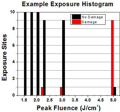
初めに、低パワー/エネルギのビームを光学素子に入射します。その光学素子の10ヶ所に1回ずつ、設定した時間(CW)またはパルス数(決められたprf)、レーザを照射します。レーザを照射した後、倍率約100倍の顕微鏡を用いた検査で確認し、すべての確認できる損傷を調べます。特定のパワー/エネルギで損傷のあった場所の数を記録します。次に、そのパワー/エネルギを増やすか減らすかして、光学素子にさらに10ヶ所レーザを照射します。このプロセスを損傷が観測されるまで繰返します。損傷閾値は、光学素子が損傷に耐える、損傷が起こらない最大のパワー/エネルギになります。1つのミラーBB1-E02の試験結果は以下のようなヒストグラムになります。
上の写真はアルミニウムをコーティングしたミラーでLIDTテストを終えたものです。このテストは、損傷を受ける前のレーザのエネルギは0.43 J/cm2 (1064 nm、10 ns pulse、 10 Hz、Ø1.000 mm)でした。
| Example Test Data | |||
|---|---|---|---|
| Fluence | # of Tested Locations | Locations with Damage | Locations Without Damage |
| 1.50 J/cm2 | 10 | 0 | 10 |
| 1.75 J/cm2 | 10 | 0 | 10 |
| 2.00 J/cm2 | 10 | 0 | 10 |
| 2.25 J/cm2 | 10 | 1 | 9 |
| 3.00 J/cm2 | 10 | 1 | 9 |
| 5.00 J/cm2 | 10 | 9 | 1 |
試験結果によれば、ミラーの損傷閾値は 2.00 J/cm2 (532 nm、10 ns pulse、10 Hz、 Ø0.803 mm)でした。尚、汚れや汚染によって光学素子の損傷閾値は大幅に低減されるため、こちらの試験はクリーンな光学素子で行っています。また、特定のロットのコーティングに対してのみ試験を行った結果ではありますが、当社の損傷閾値の仕様は様々な因子を考慮して、実測した値よりも低めに設定されており、全てのコーティングロットに対して適用されています。
CWレーザと長パルスレーザ
光学素子がCWレーザによって損傷を受けるのは、通常バルク材料がレーザのエネルギを吸収することによって引き起こされる溶解、あるいはAR(反射防止)コーティングのダメージによるものです[1]。1 µsを超える長いパルスレーザについてLIDTを論じる時は、CWレーザと同様に扱うことができます。
パルス長が1 nsと1 µs の間のときは、損傷は吸収、もしくは絶縁破壊のどちらかで発生していると考えることができます(CWとパルスのLIDT両方を調べなければなりません)。吸収は光学素子の固有特性によるものか、表面の不均一性によるものかのどちらかによって起こります。従って、LIDTは製造元の仕様以上の表面の質を有する光学素子にのみ有効です。多くの光学素子は、ハイパワーCWレーザで扱うことができる一方、アクロマティック複レンズのような接合レンズやNDフィルタのような高吸収光学素子は低いCWレーザ損傷閾値になる傾向にあります。このような低い損傷閾値は接着剤や金属コーティングにおける吸収や散乱によるものです。
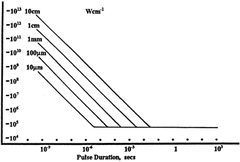
線形パワー密度におけるLIDTに対するパルス長とスポットサイズ。長パルス~CWでは線形パワー密度はスポットサイズにかかわらず一定です。 このグラフの出典は[1]です。
繰返し周波数(prf)の高いパルスレーザは、光学素子に熱的損傷も引き起こします。この場合は吸収や熱拡散率のような因子が深く関係しており、残念ながらprfの高いレーザが熱的影響によって光学素子に損傷を引き起こす場合の信頼性のあるLIDTを求める方法は確立されておりません。prfの大きいビームでは、平均出力およびピークパワーの両方を等しいCW出力と比較する必要があります。また、非常に透過率の高い材料では、prfが上昇してもLIDTの減少は皆無かそれに近くなります。
ある光学素子の固有のCWレーザの損傷閾値を使う場合には、以下のことを知る必要があります。
- レーザの波長
- ビーム径(1/e2)
- ビームのおおよその強度プロファイル(ガウシアン型など)
- レーザのパワー密度(トータルパワーをビームの強度が1/e2の範囲の面積で割ったもの)
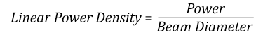
ビームのパワー密度はW/cmの単位で計算します。この条件下では、出力密度はスポットサイズとは無関係になります。つまり、スポットサイズの変化に合わせてLIDTを計算し直す必要がありません(右グラフ参照)。平均線形パワー密度は、下の計算式で算出できます。
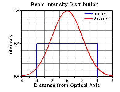
ここでは、ビーム強度プロファイルは一定であると仮定しています。次に、ビームがホットスポット、または他の不均一な強度プロファイルの場合を考慮して、おおよその最大パワー密度を計算する必要があります。ご参考までに、ガウシアンビームのときはビームの強度が1/e2の2倍のパワー密度を有します(右下図参照)。
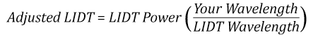
次に、光学素子のLIDTの仕様の最大パワー密度を比較しましょう。損傷閾値の測定波長が光学素子に使用する波長と異なっている場合には、その損傷閾値は適宜補正が必要です。おおよその目安として参考にできるのは、損傷閾値は波長に対して比例関係であるということです。短い波長で使う場合、損傷閾値は低下します(つまり、1310 nmで10 W/cmのLIDTならば、655 nmでは5 W/cmと見積もります)。
この目安は一般的な傾向ですが、LIDTと波長の関係を定量的に示すものではありません。例えば、CW用途では、損傷はコーティングや基板の吸収によってより大きく変化し、必ずしも一般的な傾向通りとはなりません。上記の傾向はLIDT値の目安として参考にしていただけますが、LIDTの仕様波長と異なる場合には当社までお問い合わせください。パワー密度が光学素子の補正済みLIDTよりも小さい場合、この光学素子は目的の用途にご使用いただけます。
当社のウェブ上の損傷閾値の仕様と我々が行った実際の実験の値の間にはある程度の差があります。これはロット間の違いによって発生する誤差を許容するためです。ご要求に応じて、当社は個別の情報やテスト結果の証明書を発行することもできます。損傷解析は、類似した光学素子を用いて行います(お客様の光学素子には損傷は与えません)。試験の費用や所要時間などの詳細は、当社までお問い合わせください。
パルスレーザ
先に述べたように、通常、パルスレーザはCWレーザとは異なるタイプの損傷を光学素子に引き起こします。パルスレーザは損傷を与えるほど光学素子を加熱しませんが、光学素子から電子をひきはがします。残念ながら、お客様のレーザに対して光学素子のLIDTの仕様を照らし合わせることは非常に困難です。パルスレーザのパルス幅に起因する光学素子の損傷には、複数の形態があります。以下の表中のハイライトされた列は当社の仕様のLIDT値が当てはまるパルス幅に対する概要です。
パルス幅が10-9 sより短いパルスについては、当社の仕様のLIDT値と比較することは困難です。この超短パルスでは、多光子アバランシェ電離などのさまざまなメカニクスが損傷機構の主流になります[2]。対照的に、パルス幅が10-7 sと10-4 sの間のパルスは絶縁破壊、または熱的影響により光学素子の損傷を引き起こすと考えられます。これは、光学素子がお客様の用途に適しているかどうかを決定するために、レーザービームに対してCWとパルス両方による損傷閾値を参照しなくてはならないということです。
| Pulse Duration | t < 10-9 s | 10-9 < t < 10-7 s | 10-7 < t < 10-4 s | t > 10-4 s |
|---|---|---|---|---|
| Damage Mechanism | Avalanche Ionization | Dielectric Breakdown | Dielectric Breakdown or Thermal | Thermal |
| Relevant Damage Specification | No Comparison (See Above) | Pulsed | Pulsed and CW | CW |
お客様のパルスレーザに対してLIDTを比較する際は、以下のことを確認いただくことが重要です。
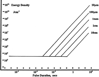
エネルギ密度におけるLIDTに対するパルス長&スポットサイズ。短パルスでは、エネルギ密度はスポットサイズにかかわらず一定です。このグラフの出典は[1]です。
- レーザの波長
- ビームのエネルギ密度(トータルエネルギをビームの強度が1/e2の範囲の面積で割ったもの)
- レーザのパルス幅
- パルスの繰返周波数(prf)
- 実際に使用するビーム径(1/e2 )
- ビームのおおよその強度プロファイル(ガウシアン型など)
ビームのエネルギ密度はJ/cm2の単位で計算します。右のグラフは、短パルス光源には、エネルギ密度が適した測定量であることを示しています。この条件下では、エネルギ密度はスポットサイズとは無関係になります。つまり、スポットサイズの変化に合わせてLIDTを計算し直す必要がありません。ここでは、ビーム強度プロファイルは一定であると仮定しています。ここで、ビームがホットスポット、または他の不均一な強度プロファイルの場合を考慮して、おおよその最大パワー密度を計算する必要があります。ご参考までに、ガウシアンビームのときは一般にビームの強度が1/e2のときの2倍のパワー密度を有します。
次に、光学素子のLIDTの仕様と最大エネルギ密度を比較しましょう。損傷閾値の測定波長が光学素子に使用する波長と異なっている場合には、その損傷閾値は適宜補正が必要です[3]。経験則から、損傷閾値は波長に対して以下のような平方根の関係であるということです。短い波長で使う場合、損傷閾値は低下します(例えば、1064 nmで 1 J/cm2のLIDTならば、532 nmでは0.7 J/cm2と計算されます)。
波長を補正したエネルギ密度を得ました。これを以下のステップで使用します。
ビーム径は損傷閾値を比較する時にも重要です。LIDTがJ/cm2の単位で表される場合、スポットサイズとは無関係になりますが、ビームサイズが大きい場合、LIDTの不一致を引き起こす原因でもある不具合が、より明らかになる傾向があります[4]。ここで示されているデータでは、LIDTの測定には<1 mmのビーム径が用いられています。ビーム径が5 mmよりも大きい場合、前述のようにビームのサイズが大きいほど不具合の影響が大きくなるため、LIDT (J/cm2)はビーム径とは無関係にはなりません。
次に、パルス幅について補正します。パルス幅が長くなるほど、より大きなエネルギに光学素子は耐えることができます。パルス幅が1~100 nsの場合の近似式は以下のようになります。
お客様のレーザのパルス幅をもとに、光学素子の補正されたLIDTを計算するのにこの計算式を使います。お客様の最大エネルギ密度が、この補正したエネルギ密度よりも小さい場合、その光学素子はお客様の用途でご使用いただけます。ご注意いただきたい点は、10-9 s と10-7 sの間のパルスにのみこの計算が使えることです。パルス幅が10-7 sと10-4 sの間の場合には、CWのLIDTも調べなければなりません。
当社のウェブ上の損傷閾値の仕様と我々が行った実際の実験の値の間にはある程度の差があります。これはロット間の違いによって発生する誤差を許容するためです。ご要求に応じて、当社では個別のテスト情報やテスト結果の証明書を発行することも可能です。詳細は、当社までお問い合わせください。
[1] R. M. Wood, Optics and Laser Tech. 29, 517 (1997).
[2] Roger M. Wood, Laser-Induced Damage of Optical Materials (Institute of Physics Publishing, Philadelphia, PA, 2003).
[3] C. W. Carr et al., Phys. Rev. Lett. 91, 127402 (2003).
[4] N. Bloembergen, Appl. Opt. 12, 661 (1973).
| Posted Comments: | |
user
(posted 2024-03-02 12:32:33.25) looking for dichroic beam splitters:
1. 1525nm(R) 1535nm(T)
2. 1550nm (R) 1535 nm(T)
3. 1565nm(R) 1550nm(T) jdelia
(posted 2024-03-05 03:10:27.0) Thank you for contacting Thorlabs. We unfortunately do not currently offer any dichroics that match these specifications. We apologize for the inconvenience. I have reached out to you directly to discuss alternative options. jw pieterse
(posted 2023-08-07 08:57:17.727) customer inspiration? : design or modify a coating that covers AR 1030-1064nm. right now your products offer one or the other. :( cdolbashian
(posted 2023-08-16 11:36:26.0) Thank you for reaching out to us with this request. I have submitted this request internally as a prospective future coating range, though in the meantime, it seems like the 1064nm V-coating could potentially work for your application, depending on how strict your requirements are for AR performance. I have reached out to you directly to share some data and discuss your intended usage. Bart Tromp
(posted 2023-02-21 17:35:14.37) However, even with adding the THORABHI.zec and THORABLO.zec coatings I cannot reproduce the numbers attained from the transmission graphs of the AB doublets (https://www.thorlabs.com/newgrouppage9.cfm?objectgroup_id=12767). The values I attain in zemax at 435nm are near 0.95 transmission. The values listed on the AB page are closer to 0.86 for this wavelength. Where does this discrepency come from? cdolbashian
(posted 2023-04-03 12:18:46.0) Thank you for reaching out to us with this inquiry. After sharing the proper way to implement such files into OpticStudio, I was able to assist you in finding the proper values we predict. Bart Tromp
(posted 2023-02-21 17:23:09.82) What is the differnce between the THORABLO & THORABHI coating files? cdolbashian
(posted 2023-04-03 12:23:25.0) Thank you for the feedback. The difference between these files is the index in which the prescription data is applied. The THORABHI should be used with glass with n > 1.6 and THORABLO should be used with glass n <1.6. Nick Taylor
(posted 2023-02-09 14:13:14.347) Hello,
I'm looking to acquire two sets of cavity ring down mirrors. One set with a center wavelength of 368 nm and the second with a center wavelength of 618 nm.
Both with a reflectivity of 99.98% and a radius of curvature of 0.5 meters (50 cm).
Is this something within your capabilities?
thanks,
nick cdolbashian
(posted 2023-02-17 11:16:37.0) Thank you for reaching out to us with this inquiry. While our standard mirrors tend to have 90-99% reflectivity within certain ranges, we do offer high reflectivity "Super mirrors" here: https://www.thorlabs.com/newgrouppage9.cfm?objectgroup_id=14069.
While they are notably more expensive, their performance is phenomenal. I have contacted you directly to discuss your application and its requirements. Ondrej Novak
(posted 2022-07-05 09:19:44.643) Dear colleagues, may I please ask what the reflectance at 1300nm for B coating is? Also, have you measured the damage threshold in W/cm2?
Thank you,
Ondrej ksosnowski
(posted 2022-07-06 12:42:32.0) Hello Ondrej, thanks for reaching out to Thorlabs. 1300nm is outside the specified range for the -B coating so it may vary between lots, however we expect the reflectance to be >3%. We have tested the CW linear damage threshold at >82 kW/cm to best scale to other beam sizes. The areal density limit can differ across beam sizes. You can view our Webinar on Laser Induced Damage for more info on the difference between these two units: https://www.youtube.com/watch?v=n0Z53O8BSI8. This topic is covered around 8 minutes in. Carme Arnalot
(posted 2022-01-26 06:07:41.25) I would like to know if you can coat our glass sensors with a spacific UV optical gel. The size of the coating is
29*14*0.2 mm. Flatness, stiffness are strict constrains.
Thanks in advance cdolbashian
(posted 2022-01-31 05:13:56.0) Thank you for contacting us at Thorlabs Carme! I have reached out to you directly to discuss the feasibility of this type of custom. In the future, please feel free to reach out to Techsales@thorlabs.com for inquiries regarding custom solutions. Damien Raynal
(posted 2021-12-10 19:37:11.313) Hello, would it be possible to know the reflectance of your C coating at 532 nm ? Thank you very much ! YLohia
(posted 2021-12-14 01:27:06.0) Hello, thank you for contacting Thorlabs. Extended range data can be requested by emailing techsupport@thorlabs.com. I have reached out to you directly with some data. Florian Sterl
(posted 2021-11-01 05:47:27.793) Hello, I am trying to model the transmission of a train of lenses in Zemax OpticStudio. In the internal coating catalog that came with the Zemax installation, I can find the Thorlabs A- and B-coatings (THORA and THORB), but not the AB-coating. In the Zemax catalog I downloaded from the Thorlabs website, I can find a 'THORABHI' and a 'THORABLO' coating. However, when I open the .zar-file of an AB-coated lens, it only shows 'AR' as the coating. Can you tell me what is the difference between these coating datasets and how to determine which is the correct one?
Thank you very much in advance! YLohia
(posted 2021-11-12 02:59:04.0) Hello, thank you for your feedback and bringing this to our attention! The -AB doublets should all be using the THORABLO and THORABHI coatings in the Zemax files. At the time the lenses were released, we mistakenly kept the coating as AR, which is just a theoretical quarter wave coating at the primary wavelength of the lens file. This should be now corrected in the web download for our Zemax catalog. user
(posted 2021-05-31 09:30:10.393) Hello,
Would you happen to have the AOI dependence for the A coating? YLohia
(posted 2021-06-04 10:12:25.0) Hello, thank you for contacting Thorlabs. I have reached out to you directly with some data. Malcolm Watson
(posted 2021-04-22 09:23:53.17) Hi, we bought an aspheric lens from you recently, which was the same type as a lens bought about 8 or 9 years ago. Both were specified as coated with the C AR coating - however, the visible colours reflected from each look very different (i.e. blue and orange, versus yellow and purple). Can you advise as to a) whether this is expected, b) whether the formulation for the C-coating has changed over the years, or c) whether it's more likely to be the wrong coating that was sent to us? We haven't yet been able to test it to check transmitted/reflected powers. Thanks, Malcolm YLohia
(posted 2021-04-22 02:08:54.0) Hello Malcolm, thank you for contacting Thorlabs. We generally don't suggest judging the coating range and performance from the color of the lens alone, especially for the -C coatings which are not designed for the visible region. Over the years, this coating has been produced in more than one chamber, so the apparent performance at non-design wavelengths (the visible range in this case) can change over different production runs. While it’s possible that this is the wrong coating, it's significantly more likely that the difference stems from run-to-run variation or a slightly different design, given that there was an eight year gap in the production of the two pieces you're comparing. We suggesting testing this part for transmission/reflection in the specified operating wavelength range. I have reached out to you directly to discuss this further. Enrique Garcia Caurel
(posted 2021-02-22 10:23:31.117) Hi,
I'd like to ask you about the possibility of manufacturing a semireflecting metal mirror deposited on a typical BK7 or silica substrate (1' or 2'). My goal is to reflect infrared reflection from 12 to roughly 5 microns and to transmit visible light, typically between 800 - 400 nm. I do not require a perfect transmission of all wavelengths in the visible, just to guarantee a good reflection of the IR (> 60%). The beam will impinge the device at an angle of incidence of 45°.
The optical component previously described is similar to the hot mirrors that you sell, in particular M254H45. However, concerning your standard hot mirrors, in your website you say that they reflect long wavelengths up to 1500 nm but nothing is said about the ability of these mirrors to reflect longer wavelengths. Since I'd like to reflect wavelengths from 12 to 5 microns I do not know whether your standard filters will work for my application or not.
Thank you very much for your attention and please do not hesitate to contact me to discuss.
Best regards,
Enrique YLohia
(posted 2021-03-05 09:59:44.0) Hello Enrique, custom items can be requested by using the "Request Quote" above or by emailing your local Thorlabs team (in your case, techsupport.fr@thorlabs.com). We will discuss the possibility of offering this directly. Craig Ingram
(posted 2020-09-21 03:46:47.667) Hello, I am trying to model a system using E01 and E02 coatings in Zemax but cannot find it in the catalogue. Is it available at all? Regards Craig YLohia
(posted 2020-10-02 03:32:19.0) Hello Craig, thank you for contacting Thorlabs. We don't offer Zemax files for these coatings because the –E0x series of mirrors have been coated in a variety of different ways over time, which means that the performance could vary significantly from one production lot to the next. We only test to ensure that the minimum reflectance spec is met for a particular wavelength range. For modeling purposes, the Zemax MIRROR surface can be used. Kathy Creath
(posted 2020-07-31 19:53:57.81) I noticed that the P-01 protected silver coating is not included in the Zemax Coating folder. Would like to see how it works in my Zemax design for use on a custom optic. Is it possible to get a copy of that file? nbayconich
(posted 2020-08-04 11:14:33.0) Thank you for contacting Thorlabs. I will reach out to you directly with more information regarding our -P01 coating. Irene de navas
(posted 2020-03-02 14:23:33.63) I work in ENUSA, supplier of nuclear fuel assemblies in Spain. We are looking for a material that gives the same picture as the UO2 sintered pellets that we manufacture, when inspected in the automatic visual equipment that we have (the inspection is performed with white light).
DOy you give that service, develope materials woth the same optical properties of another one, in this case UO2 sintered pellets?. If that is the case, we would be interested in receive information related to that service. Thank you and best regards. llamb
(posted 2020-03-04 08:11:44.0) Thank you for contacting Thorlabs. I have reached out to you directly to discuss your application further. Ricardo Ramirez
(posted 2019-07-23 14:26:19.017) I'm wondering if you have the capability to produce a metallic coating on a polycarbonate window (.236 inch thick 4 feet in diameter). YLohia
(posted 2019-07-23 03:51:40.0) Hello, I have reached out to you directly regarding this. Custom items can be requested by emailing techsupport@thorlabs.com. gsimpson
(posted 2019-01-30 12:00:03.84) We need to deliver 1064 and 532 nm light through a 6-element lens set. The very best coating is clearly the V-coating for the YAG harmonics, but it is only available for the planoconvex lenses. We also have two plano-concave , a bi-convex, and a mesiscus lens we need to integrate.
1. Can these be purchased with the V-coating, and if so at what price?
2. Can we track down data on the anticipated losses using the A or C coatings? The available spectral windows online do not include both the lowest YAG harmonics in the curves.
Thanks,
Garth YLohia
(posted 2019-01-30 03:21:03.0) Hello Garth, thank you for contacting Thorlabs. Custom coatings on our optics can be requested by emailing techuspport@thorlabs.com. We will reach out to you with information about this and the extended transmission plots for the A and C coatings. blanch
(posted 2018-12-14 14:47:07.61) To whom it may concern,
I am working at IFAE, a laboratory on particle physics in Barcelona (Spain), where we develop instrumentation of scientific instruments. We currently need a photo sensitive device that reflects less than 0.5-1% of 1064 nm light. For that the 1064 nm Antireflection Coating may nicely work.
The final goal is to allow most of the light pass and then trap to avoid 1064 nm light is reflected back. In this sense the material where the coating is made is relevant. We need a kind of filter, we do not need a lens. Can you provide information on which options are in terms of the material?
Concerning dimension, we have not them fixed but they would be at the level of few cm squares.
Additionally, the element will need to be in vacuum (10-9) and high temperatures (150 degrees).So, if you have information on that is also important.
Thanks,
Oscar llamb
(posted 2018-12-18 10:19:26.0) Hello Oscar, thank you for your feedback. In terms of vacuum compatibility, we do not test our parts beyond 10^-8 Torr, where our vacuum viewports are certified. While we cannot comment on behavior at 10^-9 Torr, we do not expect any issues at that lower pressure for our dielectric optical coatings. As for 150°C temperatures, we also would not expect any issues with our dielectric coatings, as long as the temperature is kept at a consistent temperature rather than cycled high and low. It sounds like a notch filter could be most useful for you to "trap" 1064 nm wavelengths after passing through the AR coating. I will reach out to you directly to discuss your application further. j.kurtz
(posted 2018-09-09 17:19:55.253) I would like to know what materials are used in your broad-band AR coatings. I'm particularly interested in the materials in the AR-B coating for purposes of evaluating their compatibility with the low-earth orbit environment. Cheers, Joe nbayconich
(posted 2018-09-14 02:47:12.0) Thank you for contacting Thorlabs. Unfortunately the materials used in our coating designs are proprietary information. I will reach out to you directly to discuss your application. wandner
(posted 2018-08-13 14:14:04.123) Sehr geehrte Damen und Herren,
ich wäre Ihnen sehr dankbar, wenn Sie mir mitteilen könnten, wie sich A AR-Coating im Bereich 800 bis 1000 nm verhält.
Viele Grüße
Karl Wandner swick
(posted 2018-08-28 05:13:34.0) This is a response from Sebastian at Thorlabs. Thank you for the inquiry.
I contacted you directly with the data requested.
(Ich habe Sie kontaktiert und die angefragten Daten zugeschickt.) ismael
(posted 2018-07-23 07:22:03.26) Hi, I am modeling the SOLIS3C source in Zemax and I wanted to know how to model the scattering properties of the frontal face of said source. Is there a particular black coating to use for this purposes? thanks. nreusch
(posted 2018-07-27 07:33:55.0) This is a response from Nicola at Thorlabs. Thank you for your inquiry. For analyzing the scattering properties for our SOLIS LEDs, we recommend to use a tool called LensMechanix that comes with different scattering profiles. However, Zemax OpticStudio also provides different materials as well as a coating file that could be used and edited. SOLIS LEDs contain different materials at the front face of the housing. The choice of the best suited coating therefore depends on the exact part of the housing you would like to model. We will contact you directly to provide further assistance. vitaly.tsukanov
(posted 2018-07-17 14:10:14.873) Dear Thorlabs!
Can you provide the band-pass filter interference coatings on the surfaces with high positive curvature, for example, sphere or hemisphere? The transmission features of this coating should be even over all sphere/hemisphere.surface.
thank you in advance!
Vitaly Tsukanov. YLohia
(posted 2018-07-17 10:13:50.0) Hello Vitaly, thank you for contacting Thorlabs. One thing to note is that these coatings are designed for specific AOIs since the performance is dependent on that. With a spherical design, the AOIs will be all over the place. We will reach out to you directly via email to discuss this further. v.t.tenner
(posted 2018-01-16 13:48:16.467) I am designing a broad-band optical system, with wavelengths between 300 and 1000nm. Do you have specifications of the B coating in the wavelength range between 300 and 650 nm, and for the A coating in the wavelenght range of 650-1000nm? tfrisch
(posted 2018-01-16 10:13:57.0) Hello, thank you for contacting Thorlabs. While we don't specify the out-of-band performance of our AR coatings, I'd expect over such a large range that there would be significant reflection peaks. These would change from one coating run to another, but I would not be surprised to see peaks of 10-40% at some out-of-band wavelengths. Uncoated optics may be better for your application. I will reach out to you with more details. drvanaidu
(posted 2017-12-12 20:32:48.147) hello sir, Thor labs optical coatings are very nice and useful information. plz tell me how to design and what materials are required for HR COATINGS nbayconich
(posted 2017-12-13 05:19:15.0) Thank you for contacting Thorlabs. Unfortunately our coating designs are proprietary information. Dielectric reflective coatings consist of multiple layers of varying high and low refractive indexes. The coatings are created by stacking different dielectric materials on top of one another and the thickness of these layers and number of layers create the reflectivity at a specified design wavelength range. moonbs21
(posted 2017-05-15 16:47:32.117) I appreciate your delicate products.
Can you provide dielectric coated "glass slide" and "cover slip"?
Thank you. tfrisch
(posted 2017-05-19 03:21:21.0) Hello, thank you for contacting Thorlabs. We can offer many different coatings for different substrates. I will reach out to you about the needs of your application. kritter
(posted 2017-01-27 15:07:53.123) If I cement an optical window with a C coating to another element using Norland NOA 60, what will be the reflection at the coating/cement interface at 1550nm? tfrisch
(posted 2017-02-16 02:39:38.0) Hello, thank you for contacting Thorlabs. All of our anti-reflection coatings are designed for a glass-air interface, and using an adhesive like NOA60 on the surface would disrupt that design. It would not continue to function as an anti-reflective coating. I will reach out to you directly to discuss this. kirill.gapanovich
(posted 2017-01-09 13:20:55.42) Kind Thorlabs, is it possible to receive from you coating files for LightTools? Or, if it is not possible to provide coating data for LightTools, could you please provide table data for THORA and THORB coatings, and I will make coating files by myself. tfrisch
(posted 2017-01-09 02:00:37.0) Hello, thank you for contacting Thorlabs. Unfortunately, the prescriptions of our AR coatings are proprietary, and we are unable to provide the tabular data or a model for them. You can however use the typical reflectance curves we give as a guide. I will reach out to you directly. ck.chew
(posted 2016-10-17 16:28:29.11) Could Thorlabs provide AR coating 'C' 1050-1700nm
service for Asperic Lens ACL25416U? If yes,
1. how much for ACL25416U-C?
2. MOQ?
Rgds,
CK Chew jlow
(posted 2016-10-18 04:31:43.0) Response from Jeremy at Thorlabs: I will contact you directly about this. mchen
(posted 2016-07-21 10:38:25.673) Hi, Can you do D and F AR coating on AgGaSe2 crystal? Thanks, Mike Lev.F
(posted 2016-06-26 06:41:41.553) Dear Thorlabs, we are looking optical windows operated at 900+/-20nm wavelength with 60+/-5 degrees AOI. Would you please give us transmission
curves for s- and -p polarization components for your BB AR B-coating on N-SF11 glass? This coating is used for your Anamorphic Prisms.
Thank you! peter
(posted 2016-06-22 08:45:49.803) Dear Thorlabs, what is the reflectance of the lens with C coating for wavelength 850 nm? Thank you! besembeson
(posted 2016-06-22 12:09:47.0) Response from Bweh at Thorlabs USA: You could have as much as 18% loss in reflection from each surface from the antireflection coating. Please contact me at techsupport@thorlabs.com for a typical reflectivity data of the AR coating outside its design range. cf1546
(posted 2015-01-30 09:12:35.8) Dear Thorlabs team,
in the HR coating tab you state the materials of the overcoat of protected silver (SiO2) and UV-enhanced aluminum (MgF2), but not of the protected gold. Due to material compatibility considerations, it would be nice if you could tell me
i) if the overcoat of protected gold mirrors is the same / comparable to the one of protected silver in material and deposition method (EBD?), and
ii) if there are any fluorine-containing chemical compounds like MgF2 present in protected silver or gold mirrors. Thank you! myanakas
(posted 2015-03-30 10:43:08.0) Response from Mike at Thorlabs: Thank you for your feedback. We are currently unable to specify the exact composition of the overcoat on our gold coated surface. hha07
(posted 2014-09-24 14:29:09.29) The raw data xlsx file supplies reflectivities for the various HR coatings. What polarization and angle was used for this data or is it an average?
Specifically I am worried about the reflectivity at 8 degree and 45 degree for wavelengths at the edge of the range for E02 at e.g. 397 and 866 nm. besembeson
(posted 2014-10-23 02:12:49.0) Response from Bweh: These plots and data, with the polarization states and incidence angles specified for 355nm to 920nm can be found at the following link: http://www.thorlabs.com/newgrouppage9.cfm?objectgroup_id=139&tabname=Reflectance%20Plots magnus.schloesser
(posted 2014-05-07 12:52:19.963) In our optical setup we observed laser induced contamination on half-wave plates (WPMQ05M-532). The power density on the optic was about 30 W/cm².
All other components (N-BK7 lenses, Glan-Taylor polarizer, Mirrors, ...) do not show these contaminations.
We assume that this may be related to different "chemical reactions" on the different coating surfaces of the optics.
Could you tell us the production methods (EBD, IAD, ...) of the WPMQ05M-532, a BBAR - A and a HR E02 coating? What is the material is forming the most outer layer (being the one in contact with the ambient air.)?
Thanks in advance! jlow
(posted 2014-06-12 02:08:48.0) Response from Jeremy at Thorlabs: We have not seen this issue before and we use similar coatings on other optic parts. It would be good to see if cleaning the surfaces of the wave-plates would remove this issue you are having. I will contact you directly to get more detail on this. J.Boterman
(posted 2013-11-27 10:40:28.703) Is data available on the AR-B coating for wavelengths outside the nominal range? tcohen
(posted 2013-12-05 02:52:43.0) Response from Tim at Thorlabs: Thanks for your inquiry. There will be variations in coating runs but we can supply representative out of band data. I've emailed you to discuss your wavelengths. andrea.farina
(posted 2013-09-11 13:35:17.94) Kind Thorlabs,
is it possible to have the COATING file for ZEMAX for simulation fo your lenses? If I open a lens file ZMX provided by you the program tell me that is no present the file COATINGTHOR. Can I have it?
thank you again
Andrea Farina jlow
(posted 2013-09-11 09:05:00.0) Response from Jeremy at Thorlabs: We now supply both the ZAR file and the ZMX file. The ZAR file provides you with the ZMX file as well as any supporting files. This includes the coating file. You will not run into that issue with the use of the ZAR file. jlow
(posted 2012-09-28 09:16:00.0) Response from Jeremy at Thorlabs: Our dichroic coating are designed to be used in air/vacuum. Therefore, putting the coating in direct contact would produce a significant difference in performance. franxm
(posted 2012-09-20 16:27:40.0) In general, do you expect a significant difference in dichroic coating performance if the coated side of the substrate is placed in contact with a material with a refractive index ~2? bdada
(posted 2012-04-23 17:00:00.0) Response from Buki at Thorlabs:
Thank you so much for your feedback. We are expanding our manufacturing capabilities and hope to be able to communicate a coating schedule in the future. Till then, you can request custom coated optics by emailing TechSupport@thorlabs.com. pkeesser
(posted 2012-04-20 15:18:06.0) There is really great, can we see a coating schedule thta would show available slots? |