 Products Home / 半導体レーザ用電流コントローラ(LDドライバ)、温度コントローラ、LDマウント / 組み込み用半導体レーザー(LD)ドライバー/コントローラー / 組み込み用VCSELドライバー
組み込み用VCSELドライバー
- For VCSEL Diodes
- Designed to Supply Low Drive Current
- Enhanced Safe Operation of VCSEL Diodes
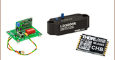
VLDC002
VITC002


Please Wait
特長
- 定電流モードで動作
- 変調入力端子付き
- 掃引の用途向けに内部三角波変調付き
- 低ノイズ出力ステージ
- レーザ電流、レーザ電流リミット、モニタ用フォトダイオード電流を制御するためのアナログ出力端子
- 標準サーミスタによるレーザ温度制御(VITC002のみ)
- サーミスタ抵抗値を設定/測定するためのアナログ出力端子(VITC002のみ)
- 2つのバージョンをご用意:
- VLDC002: 温度コントローラ無しのOEM用VCSELドライバ、ボード上にTO-46ソケット有
- VITC002: 温度コントローラ付きのOEM用VCSELドライバ、ボード上にTO-46と TO-5のソケット有
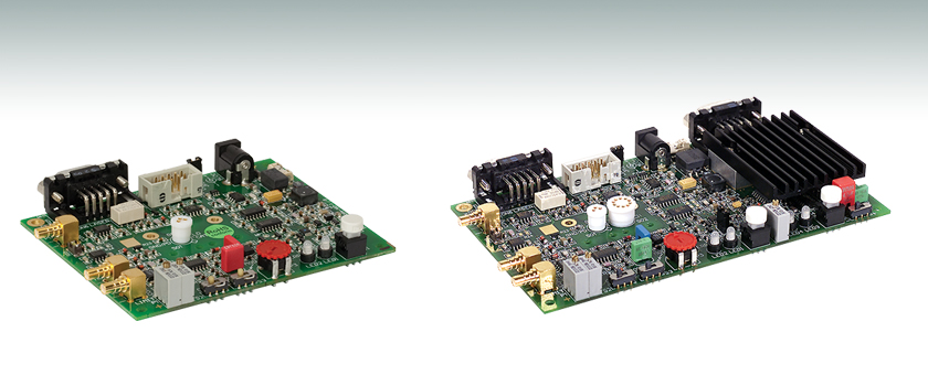
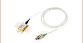
VLDC002とVITC002は、コンパクトで使い易いVCSEL(垂直共振器面発光レーザ)用のレーザ電流コントローラです。これらのコントローラは、VCSELにおいて特長的な、低い駆動電流供給用に設計されました。この製品は、実験セットアップを柔軟に構築する用途だけではなく、製品組み込み用途にも適しています。汎用の5V DC電源が付属しています。
機能性
これらのドライバには、基板上に取り付けられたTO型ソケットがあり、これにVCSELを直接プラグインすることができます。電流を三角波に変調する機能も内蔵されているので、分光測定のための高速波長掃引が実現できます。一方で、アナログ入力端子を用いて、外部からの波長変調も可能です。変調電流の上限が調整できるので、これらの機能の利用中に誤って半導体レーザを損傷することはありません。
安全なVCSEL 動作
多様な保護機能があるので、最大25 mA までのVCSELを安全で簡単に駆動できます。この製品では、非常に敏感なVCSELの損傷を予防する為に、確実に低ノイズな駆動電流が供給できるよう細心の注意が払われています。VCSELの動作温度が適切な動作温度範囲から逸脱すると、温度ウィンドウのLED表示によって望ましくない波長シフトが発生した可能性があることをお知らせします(VITC002のみ)。オープン回路の出力検知と接触不良による損傷を防ぐインターロックが、敏感なVCSEL動作の安全性を向上させます。
| 特にご注意ください: 駆動対象となるVCSELの極性を必ずご確認ください。VCSEL電流電源の極性は、AG (アノード接地) で決まっており変更できません。これらのドライバは、VCSELレーザとピン配置が同じ VCSEL以外は駆動できません。VLDC002は、VCLレーザーシリーズ用に設計されていますが、VITC002 は、VCLとVCTの両方のレーザーシリーズに対応しています。さらに詳しい情報については、 VLDC002 またはVITC002 の操作マニュアルをご参照していただくか、当社までご連絡ください。 |
| Specification for VLDC002 and VITC002 | |
|---|---|
| Current Control | |
| Laser Diode Polarity | Anode Grounded (AG), Fixed |
| Current Range | 0 - 25 mA |
| Compliance Voltage | >5 V |
| Noise | <0.8 µA Typical |
| Drift (24 hours at Constant Ambient Temperature) | <5 µA |
| Temperature Coefficient | ≤± 50 ppm/°C |
| Current Limit | 0 - 25 mA |
| Internal Triangular Modulation | |
| Frequency Range | 1 Hz - 10 kHz |
| Amplitude | 0 - 25 mA |
| Modulation Depth | 90% Typical |
| Balance Rise / Fall | 50% Typical |
| Analog Modulation Input | |
| Frequency Range (-3 dB) | DC - 100 kHz |
| Input Voltage Range | 0 - 2.5 V |
| Input impedance | 10 kΩ |
| Modulation Coefficient | 10 mA/V ± 5% |
| Photodiode Input | |
| Input Current Range | 0 to ± 2.5 mA |
| Input Impedance | Virtual Ground |
| Control Outputs | |
| Set Laser Current | 0 - 2.5 V |
| Actual Laser Current | 0 - 2.5 V |
| Photodiode Current | 0 to ±2.5 V |
| Minimum Load Resistance for Rated Accuracy | 1 MΩ |
| Accuracy (f.s.) | ±1% |
| Connectors | |
| Laser Socket | 3-pin on 2.54 mm Diameter Circle 10-pin on 5.84 mm Diameter Circle (VITC002 only) |
| Laser / Photodiode / Interlock | D-Sub 9 Pin, Female |
| Modulation Input | SMB |
| PD Input | SMB |
| TEC Element / Thermistor (VITC200 Only) | D-Sub 9 Pin, Male |
| General Data | |
| Power Supply Requirement | 5 VDC ± 5%, Regulated, 350 mA (VLDC002), 1.3 A (VITC002) |
| Included Wall Power Supply | 90 ... 264 VAC / 5 VDC |
| Current Requirement | 350 mA (VLDC002), 1.3 A (VITC002) |
| Operating Temperature | 0 - 40 °C |
| Storage Temperature | -40 - 70 °C |
| Dimensions PCB (W x D) | VLDC002: 80 mm x 100 mm VITC002: 80 mm x 140 mm |
| Dimensions Overall (W x D x H) | VLDC002: 87 mm x 105 mm x 17 mm VITC002: 87 mm x 145 mm x 17 mm |
| Additional Specifications only for VITC002 | |
|---|---|
| Temperature Control | |
| TEC Current | 0 to ±0.2 A / ±0.8 A (Selectable) |
| TEC Voltage | >2.5 V |
| Max. TEC Power | >2 W |
| Noise and Ripple | <1 mA Typical |
| TEC Current Limit | 0.2 A / 0.8 A Typical (Selectable) |
| Temperature Sensor | |
| Thermistor Control Range | 5 to 20 kΩ |
| Accuracy (f.s.) | 2% Typical |
| Stability | 2 Ω |
| Reproducibility | ±0.1% |
| Temperature Window | ±0.5 kΩ Typical |
| Control Outputs | |
| Set Thermistor Resistance | +0.5 to +2.5 V |
| Actual Thermistor Resistance | +0.5 to +2.5 V |
| Included Parts | ||
|---|---|---|
| VLDC002 | VITC002 | Part |
| x | OEM VCSEL Driver with Temp. Controller, TO-46 Socket on Board (VLDC002) | |
| x | OEM VCSEL Driver with Temp. Controller, TO-46 and TO-5 Sockets on Board (VITC002) | |
| x | x | Universal Input Power Supply |
| x | x | Operating Manual |
VLDC002平面図
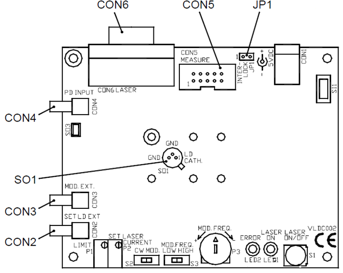
CON5-アナログおよびTTL制御用出力部
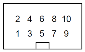
| Pin | Signal | Range |
|---|---|---|
| 1 | GND | - |
| 2 | LD ON | TTL, High when the Output is Switched On |
| 3 | ERROR | TTL, High when an Error Occurs |
| 4 | ILD SET | Set Laser Current, 100 mV/mA |
| 5 | ILD ACT | Actual Laser Current, 100 mV/mA |
| 6 | IPD | Photodiode Current, 1V/mA |
| 7...10 | Not Connected | - |
CON6-外部用半導体レーザコントロール用コネクタ
Dタイプメス型
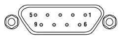
| Pin | Function | Range |
|---|---|---|
| 1 | Interlock / LED "ON" | Needs Low Ohmic Return to Pin 5 |
| 2 | Monitor Diode GND | - |
| 3 | Laser Anode, GND | - |
| 4 | Monitor Diode In | 0 ... 2.5 mA |
| 5 | Interlock / LED GND | - |
| 7 | Laser Cathode | 0 ... 25 mA |
| 6,8,9 | Not Connected | - |
| Shield | GND | - |
SO1-半導体レーザーソケット
2ピンまたは3ピンの半導体レーザ
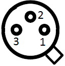
| Pin | Function |
|---|---|
| 1 | Laser Cathode |
| 2 | Laser Anode, GND |
| 3 | Laser Anode, GND |
JP1
インターロック
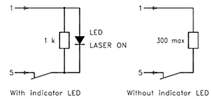
半導体レーザの出力がONであり続けるには、ピン1とピン5の間で、短絡または最小抵抗値(R<300 Ω)の維持が必要です、 また、LEDを1 kΩの抵抗器と共に使用し、2つのピンの間に並列に接続する方法もあります。レーザへの電流出力スイッチがONになれば、LEDが発光します。
CON2-SMBオス型
レーザ電流の外部設定用入力端子
CON3-SMBオス型
レーザ電流の変調用入力端子
CON4-SMBオス型
外部フォトダイオード用入力端子
VITC002平面図
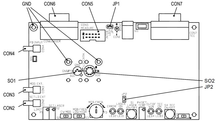
CON7 - 外部温度コントロール用コネクタ
Dタイプメス型
| PIN | Function | Range |
|---|---|---|
| 2 | Thermistor | 20 µA |
| 3 | Thermistor Ground | - |
| 4 | TEC + | -0.2 ...+0.2 A / -0.8 ... +0.8 A (selectable) |
| 5 | TEC - | +0.2 ... -0.2 A / +0.8 ... -0.8 A (selectable) |
| Shield | GND | - |
CON5 - アナログおよびTTL制御用出力部
| PIN | Signal | Range |
|---|---|---|
| 1 | GND | - |
| 2 | LD ON | TTL, High when the output is switched on |
| 3 | ERROR | TTL, High when an error occurs |
| 4 | ILD SET | Set laser current, 100 mV/mA |
| 5 | ILD ACT | Actual laser current, 100 mV/mA |
| 6 | IPD | Photodiode current, 1V/mA |
| 7 | R ACT | Actual thermistor resistance, 100 mV/kΩ |
| 8 | R SET | Set Tthermistor resistance, 100 mV/kΩ |
| 9 | OUT OF WIN | TTL, High when the thermistor resistance is out of the window |
| 10 | TEC ON | TTL, High when the temperature control is switched on |
CON6 - 外部半導体レーザコントロール用コネクタ
Dタイプメス型
| PIN | Function | Range |
|---|---|---|
| 1 | Interlock / LED "ON" | needs low ohmic return to pin 5 |
| 2 | Monitor Diode GND | - |
| 3 | Laser Anode, GND | - |
| 4 | Monitor Diode In | 0 ... 2.5 mA |
| 5 | Interlock / LED GND | - |
| 7 | Laser Cathode | 0 ... 25 mA |
| 6,8,9 | Not Connected | - |
| Shield | GND | - |
JP1
インターロック
半導体レーザの出力がONであり続けるには、ピン1とピン5の間で、短絡または最小抵抗値(R<300 Ω)の維持が必要です、 また、LEDを1 kΩの抵抗器と共に使用し、2つのピンの間に並列に接続する方法もあります。レーザへの電流出力スイッチがONになれば、LEDが発光します。
JP2
半導体レーザの温度ウィンドウ保護
ジャンパーワイヤJP2をつなげば、温度ウィンドウが保護できます。 温度ウィンドウの保護がENABLE状態の時、実際のサーミスタの抵抗値が±0.5 kΩウィンドウの範囲外である限り、半導体レーザはOFF状態になります(またはスイッチON状態になりません)。 実際の抵抗値がウィンドウの範囲になれば、すぐにレーザは再びスイッチON状態になります(もしくはスイッチONできる状態になります)。
SO1 - 半導体レーザーソケット
2ピンまたは3ピンの半導体レーザ
| Pin | Function |
|---|---|
| 1 | Laser Cathode |
| 2 | Laser Anode, GND |
| 3 | Laser Anode, GND |
CON2 - SMBオス型
レーザ電流の外部設定用入力端子
S02 - 半導体レーザーソケット
10ピンの半導体レーザ
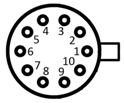
| Pin | Function |
|---|---|
| 1 | TEC + |
| 3 | Laser Cathode |
| 4 | Laser Anode, GND |
| 8 | Thermistor GND |
| 9 | Thermistor |
| 10 | TEC - |
| 2,5,6,7 | Not Used |
CON3 - SMBオス型
レーザ電流の変調用入力端子
CON4 - SMBオス型
外部フォトダイオード用入力端子
| Posted Comments: | |
Haoran Zhu
(posted 2022-10-21 14:46:40.457) hi
We have an external Laser to connect with the laserdriver(VITC002) in our Lab, and need some technik supports.
1. The Laser should working at the specific temperatur and we can calculate the resistance. the question is we should set the resistance from Laserdriver as temperatur control system. Is that p4 on the board we could direct chance to the calculated resistance? (Manual page 24/ 3.3.5 Adjusting the Thermistor set resistance)
2. as Manual page 21/ 3.3.1 Adjusting the limit. we could adjust ILimit. Is that current as same as ILD? (to ensure that the Laser LD Cathode&Anode is at a safe current.) if not what is the different between this two?
3.same, the current given to the TEC+ and TEC- ports of the Laser, also needs to be given a safe value by the driver (the maximum current of our laser TEC is 0.9A), so what components can the driver control through?
i dont know if you can solve my problem, if positiv answer thanks a lot
Haoran hkarpenko
(posted 2022-10-28 08:03:28.0) Dear Haoran,
thank you very much for your feedback. I contacted you directly to discuss this with you. Tyler
(posted 2008-10-03 09:14:29.0) A response from Tyler at Thorlabs to s.obyrne: After talking to our engineers in Germany I have some additional information. They recommend using Thorlabs benchtop controller (LDC200CV) since it was designed to allow for the operation of diodes with that pin configuration. However, if an OEM type driver is necessary, the only solution is to desolder the socket and rewire it for your pin configuration. This will potentially introduce noise into the system. The more elegant solution of altering the circuit directly is not possible because the circuit board is multilayered. Tyler
(posted 2008-09-25 09:50:11.0) A response from Tyler at Thorlabs to s.obyrne: Unfortunately, it is not reasonable to make changes to the VITC002 circuit to make it compatible with a cathode grounded VCSEL. Thank you for considering Thorlabs for you photonics needs. s.obyrne
(posted 2008-09-25 06:26:06.0) I would like to use this driver with a VCSEL from a company other than vertilas. They produce their diodes with the cathode at ground, and I understand that this circuit uses anode ground. Is there anything I can do with this circuit to allow it to work with a diode whose cathode is connected to the case and the negative TEC input?
Thanks |
半導体レーザーコントローラーセレクションガイド
下の表は、当社の半導体レーザ用コントローラおよびデュアル半導体レーザ/温度コントローラの主な仕様の一覧です。詳しい内容や仕様について、またはご注文の際には表内の型番をクリックしてご確認ください。
| Current Controllers | ||||||
|---|---|---|---|---|---|---|
| Item # | Drive Current | Compliance Voltage | Constant Current | Constant Power | Modulation | Package |
| LDC200CV | 20 mA | 6 V | External | Benchtop | ||
| VLDC002 | 25 mA | 5 V | - | Int/Ext | OEM | |
| LDC201CU | 100 mA | 5 V | External | Benchtop | ||
| LD2000R | 100 mA | 3.5 V | - | External | OEM | |
| EK2000 | 100 mA | 3.5 V | - | External | OEM | |
| LDC202C | 200 mA | 10 V | External | Benchtop | ||
| KLD101 | 230 mA | ≤10 V | External | K-Cube™ | ||
| IP250-BV | 250 mA | 8 Va | External | OEM | ||
| LD1100 | 250 mA | 6.5 Va | - | -- | OEM | |
| LD1101 | 250 mA | 6.5 Va | - | -- | OEM | |
| EK1101 | 250 mA | 6.5 Va | - | -- | OEM | |
| EK1102 | 250 mA | 6.5 Va | - | -- | OEM | |
| LD1255R | 250 mA | 3.3 V | - | External | OEM | |
| LDC205C | 500 mA | 10 V | External | Benchtop | ||
| IP500 | 500 mA | 3 V | External | OEM | ||
| LDC210C | 1 A | 10 V | External | Benchtop | ||
| LDC220C | 2 A | 4 V | External | Benchtop | ||
| LD3000R | 2.5 A | -- | - | External | OEM | |
| LDC240C | 4 A | 5 V | External | Benchtop | ||
| LDC4005 | 5 A | 12 V | Int/Ext | Benchtop | ||
| LDC4020 | 20 A | 11 V | Int/Ext | Benchtop | ||
| Dual Temperature and Current Controllers | |||||||
|---|---|---|---|---|---|---|---|
| Item # | Drive Current | Compliance Voltage | TEC Power (Max) | Constant Current | Constant Power | Modulation | Package |
| VITC002 | 25 mA | 5 V | > 2 W | - | Int/Ext | OEM | |
| ITC102 | 200 mA | > 4 V | 12 W | Ext | OEM | ||
| ITC110 | 1 A | > 4 V | 12 W | Ext | OEM | ||
| ITC4001 | 1 A | 11 V | > 96 W | Int/Ext | Benchtop | ||
| CLD1010LPa | 1.0 A | > 8 V | > 14.1 W | Ext | Benchtop | ||
| CLD1011LPb | 1.0 A | > 8 V | > 14.1 W | Ext | Benchtop | ||
| CLD1015c | 1.5 A | > 4 V | > 14.1 W | Ext | Benchtop | ||
| ITC4002QCLd | 2 A | 17 V | > 225 W | Int/Ext | Benchtop | ||
| ITC133 | 3 A | > 4 V | 18 W | Ext | OEM | ||
| ITC4005 | 5 A | 12 V | > 225 W | Int/Ext | Benchtop | ||
| ITC4005QCLd | 5 A | 20 V | > 225 W | Int/Ext | Benchtop | ||
| ITC4020 | 20 A | 11 V | > 225 W | Int/Ext | Benchtop | ||
当社では製品組み込み用あるいはラックマウントの半導体レーザ電流&温度コントローラ(組み込み用モジュール、PRO8電流コントロールモジュール、PRO8電流&温度コントロールモジュール)もご用意しております。