 Products Home
自由空間光用差分増幅フォトディテクター
- Wavelengths Covering the 190 - 1700 nm Range
- DC to 1 MHz or DC to 100 MHz Bandwidths
- Detectors with Diameters up to 5 mm
- Common Mode Rejection Ratio ≥30 dB
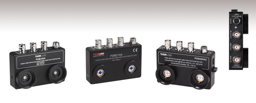
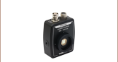
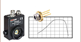
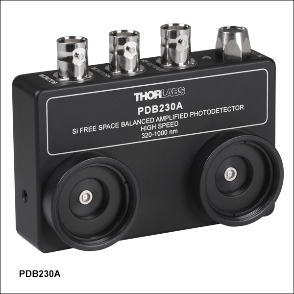
PDB230C
InGaAs Photodetector
for 800 - 1700 nm
PDB210A
Si Photodetector
for 320 - 1060 nm
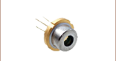
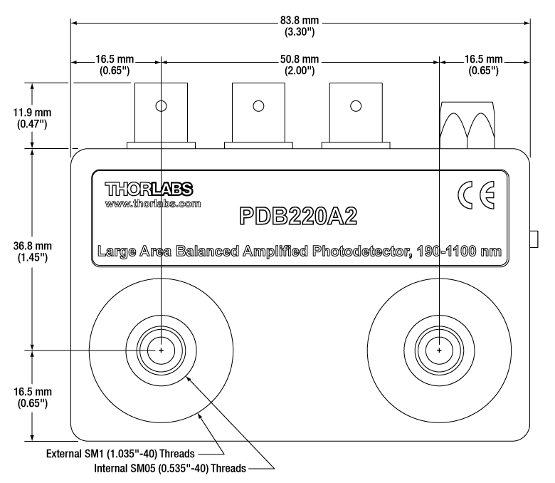
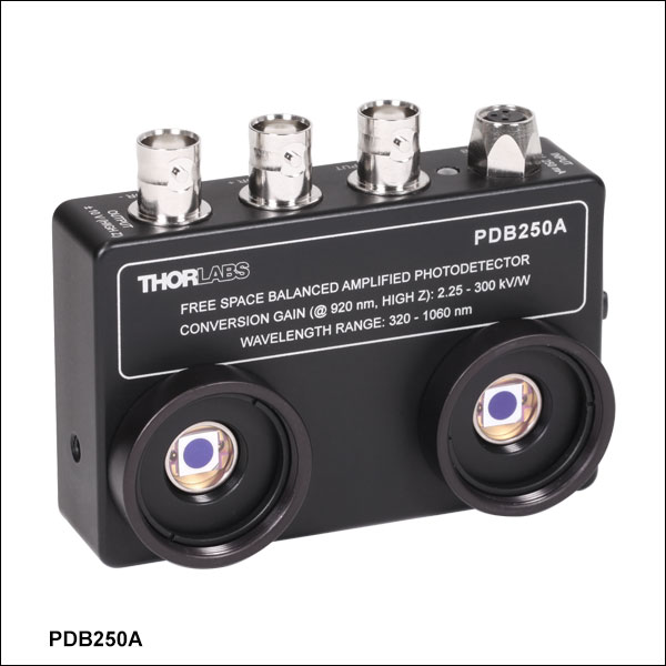
Top Panel of
the PDB250A
PDB250A2
Switchable Gain
UV-Enhanced Si Photodetector
for 190 - 1060 nm


Please Wait
| Balanced Detector Selection Guide |
|---|
| Balanced Detectors with Fast Monitor Output |
| Free-Space Balanced Amplified Detectors |
| Suitable for OCT |
| Compact Balanced Amplified Detectors |
| Compact 5 GHz Balanced Detectors |
| OCT Balanced Detectors with Fast Monitor Output |
| Auto-Balanced Detector with Avalanche Photodiodes |
| Polarization-Dependent Balanced Detector |
主な用途例
- 分光
- ヘテロダイン検出
- 光コヒーレンストモグラフィ(OCT)
- 光遅延測定
- THz検出
Click to Enlarge
フォトディテクタPDB220A2の概略外形図
特長
- コモンモード除去比: ≥30 dB
- 広い帯域幅: DC~1 MHzまたはDC~100 MHz
- 固定および切り替え可能な利得
- 利得固定タイプ: PDB220A2/M、PDB210x/M、PDB230x
- 利得切り替え可能タイプ: PDB250x
- 超低ノイズ(モデルごとのNEPは「仕様」タブ参照)
- 自由空間用途向け(ファイバ入力も可能)
- ディテクタの直接出力信号のモニタも可能
- 電源が付属
- SM1外ネジとSM05内ネジ付き
こちらの自由空間光用差分増幅フォトディテクタは、2つの光入力信号の差分をとることにより、コモンモードノイズを除去します。それにより、信号経路上の微弱な信号の変化を干渉ノイズのフロアの中から抽出することができます。フォトディテクタPDB230xは、PDB220A2/M、PDB210A/M、PDB210C/M、PDB250xに比べて受光面は小さくなっていますが、帯域幅は大きくなっています(下表をご覧ください)。
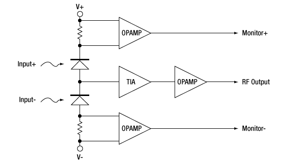
各ディテクタには、2つのよく整合されたSiまたはInGaAsディテクタと、超低ノイズのトランスインピーダンス増幅器が使用されています。出力電圧(RF-OUTPUT)は、この2つのフォトダイオードの光電流(つまり2つの光入力信号)の差に比例する信号です。PDB250xシリーズのディテクタは、利得範囲42 dBを8段階で切り替えることができます。詳細は「動作」タブをご覧ください。また、各フォトディテクタにはそれぞれ個別に高速モニタ出力(MONITOR+、MONITOR-)も付いており、それらを用いて各ディテクタの光入力のパワーレベルを個別に測定したり、各ディテクタ上のRF変調信号を測定したりできます。
2つのディテクタは50.8 mm(2インチ)離れているため、光学テーブル上でのビームのアライメントが容易です。これらのディテクタをさらに使いやすくするために、筐体には各ディテクタの周囲にSM1外ネジとSM05内ネジが付いており、レンズチューブ、ケージシステム、マウント付き光学素子、ファイバーコリメータ用アダプタなどのコンポーネントを取付けることができます。SM1外ネジ付き製品にも対応できるように、各ディテクタにはアダプタSM1T1が2個付属しています。
電気コネクタ
3つのBNCコネクタからは、2つの入射光に対するそれぞれのパワーモニタ信号と、それら2つの差分信号が出力されます。2つのモニタ信号は各チャンネル用の独立したパワーメータとして使用することができ、各フォトダイオードへの入射光のパワーレベルを調整するのに便利です。
筐体と電源
これらの差分ディテクタはシールドされたアルミ製筺体に納められています。この筐体の底部または側面にはM4 x 0.7ネジ穴があり、ポストに取り付けることができます。これらの差分ディテクタ用の電源として、±12 V DC電源LDS12Bが付属します。 電源LDS12Bは交換用として別途ご購入いただくことも可能です(下記参照)。
当社では、差分ディテクタを内蔵したファイバベースの干渉計もご用意しています。
固定式利得アダプタ
| Item #a | PDB220A2(/M) | PDB210A(/M) | PDB210C(/M) | PDB230A | PDB230C | |
|---|---|---|---|---|---|---|
| Detector Type | UV Enhanced Si/PIN | Si/PIN | InGaAs/PIN | Si/PIN | InGaAs/PIN | |
| Wavelength Range | 190 - 1100 nm | 320 - 1060 nm | 800 - 1700 nm | 320 - 1000 nm | 800 - 1700 nm | |
| Typical Maximum Responsivity @ Peak Wavelength | 0.5 A/W @ 960 nm | 0.6 A/W @ 920 nm | 1.0 A/W @ 1550 nm | 0.53 A/W @ 820 nm | 1.0 A/W @ 1550 nm | |
| Peak Wavelength | 960 nm | 920 nm | 1550 nm | 820 nm | 1550 nm | |
| Diameter of Active Detector Area | 4.1 mm | 5 mm | 3 mm | 0.8 mm | 0.3 mm | |
| Photodiode Damage Threshold | 20 mW | |||||
| Optical Input | Free-Space | |||||
| RF Output | ||||||
| Electrical Output | BNC, 100 Ω | BNC, 50 Ω | ||||
| Output Coupling | DC (AC-Coupling Available Upon Request) | |||||
| Bandwidth (3 dB) | DC - 1 MHz | DC - 100 MHz | ||||
| Common Mode Rejection Ratio (CMRR) Typical | 30 dB (Typical) | 40 dB (Typical) | 30 dB (Typical) | >30 dB 35 dB (Typical) | >30 dB 40 dB (Typical) | |
| Transimpedance Gain | High Z Load | 500 x 103 V/A | 50 x 103 V/A | |||
| 50 Ω Load | 175 x 103 V/A | 24.5 x 10³ V/A | ||||
| Conversion Gain @ Peak Wavelength | High Z Load: 250 x 103 V/W | High Z Load: 300x103V/W | High Z Load: 500 x 103 V/W | 26.5 x 10³ V/W | 50 x 103 V/W | |
| 50 Ω Load: 85 x 103 V/W | 50 Ω Load: 100 x 103 V/W | 50 Ω Load: 175 x 103 V/W | ||||
| CW Saturation Power @ Peak Wavelength | 36 µW | 33 µW | 20 µW | 150 µW | 80 µW | |
| Minimum NEP | 3.6 pW/√Hz (DC - 1 MHz) | 2.2 pW/√Hz (DC - 1 MHz) | 16 pW/√Hz (DC - 1 MHz) | 12 pW/√Hz (DC - 100 MHz) | 7.5 pW/√Hz (DC - 100 MHz) | |
| Voltage Swing | High Z Load | 10 V (Max) | ± 4.0 V | |||
| 50 Ω Load | 3.5 V (Max) | ± 1.9 V | ||||
| Typical Performance Graphsb | ||||||
| Monitor Output | ||||||
| Electrical Output | BNC, 100Ω | BNC, 50 Ω | ||||
| Conversion Gain @ Peak Wavelength | High Z Load | 10 V/mW | 10 V/mW | 10 V/mW | 10 V/mW | 10 V/mW |
| 50 Ω Load | 1.5 V/mW | 1.5 V/mW | 1.5 V/mW | - | - | |
| Voltage Swing | High Z Load | 10 V (Max) | 10 V (Max) | |||
| 50 Ω Load | 1.5 V (Max) | 1.55 V (Max) | ||||
| General | ||||||
| Operating Temperature Rangec | 0 °C to 40 °C | |||||
| Storage Temperature Range | -40 °C - 70 °C | |||||
| Dimensionsd | 83.8 mm x 65.3 mm x 21.1 mm (3.30" x 2.57" x 0.83") | 84.5 mm x 65.3 mm x 21.1 mm (3.33" x 2.57" x 0.83") | ||||
| Included LDS12B Power Supplye | ±12 V @ 250 mA (100/120/230 VAC, 50 - 60 Hz, Switchable) | |||||
利得切り替え可能なディテクタ
| Item #a | PDB250A2 | PDB250A | PDB250C | |
|---|---|---|---|---|
| Detector Type | UV Enhanced Si/PIN | Si/PIN | InGaAs/PIN | |
| Wavelength Range | 190 to 1100 nm | 320 to 1060 nm | 800 to 1700 nm | |
| Typical Maximum Responsivity @ Peak Wavelength | 0.5 A/W @ 960 nm | 0.6 A/W @ 920 nm | 1.0 A/W @ 1550 nm | |
| Peak Wavelength | 960 nm | 920 nm | 1550 nm | |
| Diameter of Active Detector Area | 4.1 mm | 5 mm | 3 mm | |
| Photodiode Damage Threshold | 20 mW | |||
| Optical Input | Free-Space | |||
| RF Output | ||||
| Electrical Output | BNC, 100 Ω | |||
| Output Coupling | DC (AC-Coupling Available Upon Request) | |||
| Bandwidth (3 dB)b | DC - 1 MHz | |||
| Common Mode Rejection Ratio Typical | 35 dB | 35 dB | 30 dB | |
| Gain Adjustment Range | 42 dB | |||
| Gain Steps | 8 | |||
| Transimpedance Gain | High Z Load | 750 V/A - 500 x 103 V/A | ||
| 50 Ω Load | 263 V/A - 175 x 103 V/A | |||
| Conversion Gain @ Gain = 8, Peak Wavelength | High Z Load | 250 x 103 V/W | 300 x 103 V/W | 500 x 103 V/W |
| 50 Ω Load | 87.5 x 10³ V/W | 105 x 103 V/W | 175 x 103 V/W | |
| Conversion Gain @ Gain = 1, Peak Wavelength | High Z Load | 1.87 x 10³ V/W | 2.25 x 10³ V/W | 3.75 x 10³ V/W |
| 50 Ω Load | 0.65 x 10³ V/W | 0.78 x 10³ V/W | 1.3 x 10³ V/W | |
| CW Saturation Power @ Gain = 1, Peak Wavelength | 5.3 mW | 4.4 mW | 2 mW | |
| Minimum NEP (DC - 1 MHz) @ Gain = 8 | 6.5 pW/√Hz | 5 pW/√Hz | 17 pW/√Hz | |
| Voltage Swing | High Z Load | ± 10 V | ||
| 50 Ω Load | ± 2.5 V | |||
| Typical Performance Graphsc | ||||
| Monitor Output | ||||
| Electrical Output | BNC, 200 Ω | |||
| Output Bandwidth (3 dB) | DC - 10 kHz | DC - 10 kHz | DC - 2 kHz | |
| Conversion Gain @ Peak Wavelength | High Z Load | 10 V/mW | 10 V/mW | 10 V/mW |
| 50 Ω Load | 2.5 V/mW | 1.5 V/mW | 1.5 V/mW | |
| Voltage Swing | High Z Load | Max. 10 V | ||
| 50 Ω Load | Max. 1.5 V | |||
| Overall Output Voltage Noise | < 0.65 mVRMS | |||
| DC Offset | < ±5 mV | |||
| General | ||||
| Operating Temperature Ranged | 5 °C - 40 °C | |||
| Storage Temperature Range | -40 °C - 70 °C | |||
| Dimensionse | 88.2 mm x 65.3 mm x 21.1 mm (3.47" x 2.57" x 0.83") | |||
| Included LDS12B Power Supplyf | ±12 V @ 250 mA (100/120/230 VAC, 50 - 60 Hz, Switchable) | |||
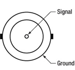
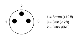
自由空間光用差分増幅フォトディテクタのピン配列
Monitor +/-
BNCメス型
PDB220A2/M、PDB210A/M、PDB210C/M、PDB250xでは、高インピーダンス負荷時: 10 V (Max)、50 Ω負荷時: 1.5 V (Max)
PDB230A、PDB230Cでは、高インピーダンス負荷時: 10 V、50 Ω負荷時: 1.55 V (Max)
RF出力端子用
BNCメス型
PDB220A2/M、PDB210A/M、PDB210C/Mでは、高インピーダンス負荷時: 10 V (Max)、50 Ω負荷時: 3.5 V (Max)
PDB250xでは、高インピーダンス負荷時: 10 V (Max)、50 Ω負荷時: 2.5 V (Max)
PDB230A、PDB230Cでは、高インピーダンス負荷時: ±4.0 V、50 Ω負荷時: ±1.9 V
電源用コネクタ メス型(フォトディテクタ)
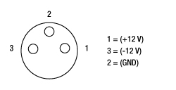
電源用コネクタ オス型(電源ケーブル)
当社の自由空間光用差分増幅フォトディテクタは、2つの整合性のとれたフォトダイオードと超低ノイズの高速トランスインピーダンスアンプ(TIA)で構成されています。TIAは2つのフォトダイオードの光電流(2つの光入力信号)の差分に比例した出力電圧(RF OUTPUT)を生成します。また、ディテクタには、それぞれ個々のフォトダイオードの入力パワーレベルを確認するために、2つの高速モニタ出力ポート(MONITOR+と MONITOR-)が付いています。
当社の自由空間光用差分増幅フォトディテクタには下記が含まれます。
フォトダイオードのチュートリアル
動作原理
接合型フォトダイオードは、通常の信号ダイオードと似た動作をする部品ですが、接合半導体の空乏層が光を吸収すると、光電流を生成する性質があります。フォトダイオードは、高速なリニアデバイスで、高い量子効率を達成し、様々な用途で利用することが可能です。
入射光の強度に応じた、出力電流レベルと受光感度を正確に把握することが必要とされます。図1は、接合型フォトダイオードのモデル図で、基本的な部品要素が図示されており、フォトダイオードの動作原理が説明されています。
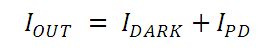
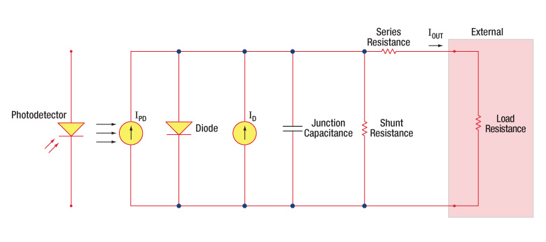
図1:フォトダイオードの概略図
フォトダイオード関連用語
受光感度
フォトダイオードの受光感度は、規定の波長における、生成光電流 (IPD)と入射光パワー(P)の比であると定義できます。
Photoconductiveモード(光導電モード)とPhotovoltaicモード(光起電力モード)
フォトダイオードは、Photoconductiveモード(逆バイアス) またはPhotovoltaicモード(ゼロバイアス)で動作できます。 モードの選択は、使用用途で求められる速度と、許容される暗電流(漏れ電流)の量で決まります。
Photoconductiveモード(光導電モード)
Photoconductiveモードでは、逆バイアスが印加されますが、これが当社のDETシリーズディテクタの基本です。回路で測定できる電流量はフォトダイオードに照射される光の量を反映します。つまり、測定される出力電流は、入射される光パワーに対しリニアに比例します。逆バイアスを印加すると、空乏層を広げて反応領域が広くなるため、接合容量が小さくなり、良好な線形応答が得られます。このような動作条件下では、暗電流が大きくなりがちですが、フォトダイオードの種類を選ぶことで、暗電流を低減することもできます。(注:当社のDETディテクタは逆バイアスで、順方向バイアスでは動作できません。)
Photovoltaicモード(光起電力モード)
Photovoltaicモードでは、フォトダイオードはゼロバイアスで使用されます。デバイスからの電流の流れが制限されると電位が上昇します。このモードでは光起電力効果が引き起こされますが、これが太陽電池の基本です。Photovoltaicモードでは、暗電流は小さくなります。
暗電流
暗電流とは、フォトダイオードにバイアス電圧が付加されている時に流れる漏れ電流です。Photoconductiveモードで使用する場合に暗電流の値は高くなりがちで、温度の影響も受けます。 暗電流は、温度が10°C上昇するごとに約2倍となり、シャント抵抗は6°C の上昇に伴い倍になります。高いバイアスを付加すれば、接合容量は小さくなりますが、暗電流の量は増大してしまいます。
暗電流の量はフォトダイオードの材料や検出部の寸法によっても左右されます。ゲルマニウム製のデバイスでは暗電流は高くなり、それと比較するとシリコン製のデバイスは一般的には低い暗電流となります。下表では、いくつかのフォトダイオードに使用される材料の暗電流の量と共に、速度、感度とコストを比較しています。
| Material | Dark Current | Speed | Spectral Range | Cost |
|---|---|---|---|---|
| Silicon (Si) | Low | High Speed | Visible to NIR | Low |
| Germanium (Ge) | High | Low Speed | NIR | Low |
| Gallium Phosphide (GaP) | Low | High Speed | UV to Visible | Moderate |
| Indium Gallium Arsenide (InGaAs) | Low | High Speed | NIR | Moderate |
| Indium Arsenide Antimonide (InAsSb) | High | Low Speed | NIR to MIR | High |
| Extended Range Indium Gallium Arsenide (InGaAs) | High | High Speed | NIR | High |
| Mercury Cadmium Telluride (MCT, HgCdTe) | High | Low Speed | NIR to MIR | High |
接合容量
接合容量(Cj)は、フォトダイオードの帯域幅と応答特性に大きな影響を与えるので、フォトダイオードの重要な特性となります。ダイオードの面積が大きいと、接合容量が大きくなり、電荷容量は大きくなります。逆バイアスの用途では、接合部の空乏層が大きくなるので、接合容量が小さくなり、応答速度が速くなります。
帯域幅と応答性
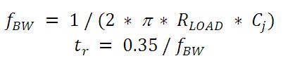
負荷抵抗とフォトディテクタの接合容量により帯域幅が制限されます。最善の周波数応答を得るには、50 Ωの終端装置を50 Ωの同軸ケーブルと併用します。接合容量(Cj)と負荷抵抗値(RLOAD)により、帯域幅(fBW)と立ち上がり時間応答(tr)の概算値が得られます。
ノイズ等価電力
ノイズ等価電力(NEP)とは、信号対雑音(S/N)比が1であるときに生成されるRMS信号電圧の値です。NEPによって、ディテクタが低レベルの光を検知する能力を知ることができるので、この数値は便利です。一般には、NEPはディテクタの検出部の面積増加に伴って大きくなり、下記の数式で求めることができます。
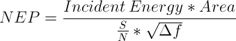
この数式において、S/Nは信号対雑音比、Δf はノイズの帯域幅で、入射エネルギ単位はW/cm2となっています。詳細は、当社のホワイトペーパー「NEP – Noise Equivalent Power」をご覧ください。
終端抵抗
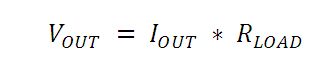
オシロスコープでの測定を可能にするためには、生成された光電流を電圧(VOUT)に変換する必要がありますが、負荷抵抗を用いて電圧変換します。
フォトダイオードの種類によっては、負荷抵抗が応答速度に影響を与える場合があります。最大帯域幅を得るには、50 Ωの同軸ケーブルを使用して、ケーブルの反対側の終端部で50 Ωの終端抵抗器の使用を推奨しています。このようにすることで、ケーブルの特性インピーダンスとマッチングできて共鳴が最小化できます。帯域幅が重要ではない特性の場合は、RLOADを増大させることで、所定の光レベルに対して電圧を大きくすることができます。終端部が不整合の場合、同軸ケーブルの長さが応答特性に対して大きな影響を与えます。したがってケーブルはできるだけ短くしておくことが推奨されます。
シャント抵抗
シャント抵抗は、ゼロバイアスフォトダイオード接合の抵抗を表します。理想的なフォトダイオードでは、シャント抵抗は無限大となりますが、実際の数値はフォトダイオードの材料の種類によって、10Ωのレベルから 数千MΩの範囲となる場合があります。例えばInGaAsディテクタのシャント抵抗は、10 MΩのレベルですが、GeディテクタはkΩのレベルです。このことは、フォトダイオードのノイズ電流に大きく影響を与える可能性があります。しかしながらほとんどの用途では、ある程度高い抵抗値であればその影響は小さく、無視できる程度です。
直列抵抗
直列抵抗は半導体材料の抵抗値で、この低い抵抗値は、通常は無視できる程度です。直列抵抗は、フォトダイオードの接触接続部とワイヤ接続部で発生し、ゼロバイアスの条件下でのフォトダイオードのリニアリティの主な決定要因になります。
一般的な動作回路
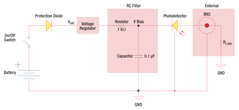
図2: 逆バイアス回路(DETシリーズディテクタ)
上図の回路はDETシリーズのディテクタをモデル化したものです。ディテクタは、入射光に対して線形の応答を得るために逆バイアス状態になっています。ここで生成された光電流の量は、入射光と波長に依存し、負荷抵抗を出力端子に接続すると、オシロスコープでモニタリングできます。RCフィルタの機能は、出力に雑音を載せてしまう可能性のある供給電力からの高周波雑音のフィルタリングです。

図3: 増幅ディテクタ回路
高利得用途でアンプとともにフォトディテクタを使用できます。動作時には、PhotovoltaicモードまたはPhotoconductiveモードのいずれも選択可能です。このアクティブ回路はいくつかの利点があります。
- Photovoltaicモード:オペアンプで、点Aと点Bの電位が同じに維持されているので、フォトダイオードでは回路全体では0 Vに保たれています。このことで暗電流は発生しなくなります。
- Photoconductiveモード: フォトダイオードは逆バイアス状態であるので、接合容量を低下させ、帯域幅の状態を改善します。ディテクタの利得は、フィードバック素子(Rf)に依存します。ディテクタの帯域幅は、下記の数式で計算することができます。
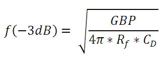
GBPが利得帯域幅積で、CDは接合容量と増幅器の静電容量の和です。
チョッパ入力周波数の影響
光導電信号は時定数の応答限界までは一定となりますが、PbS、 PbSe、HgCdTe (MCT)、InAsSbなどのディテクタにおいては、1/fゆらぎ(チョッパ入力周波数が大きいほどゆらぎは小さくなる)を持つため、低い周波数の入力の場合は影響が大きくなります。
低いチョッパ入力周波数の場合は、ディテクタの受光感度は小さくなります。周波数応答や検出性能は下記の条件の場合において最大となります。
![]()
| Posted Comments: | |
baolong zhang
(posted 2023-08-28 11:38:20.81) Dear Sir or Madam,
I have a problem about the product PDB210A/M,
This balance detector have 3 output, "+" , "-" , and "RFoutput".
When I try to measure the channel "+" or "-" by an osilloscope at the condition that block one of this sensor and the power is on.
And I found that the blocked channel always have some signal comparible to the unblocked channel.
see picture below:
【no photo here】
the green line is the signal connected to blocked channel, it is not only have some signal but also distorted.
This weird phenomenon affect my measurement, is there any way that i can fix this?
Looking forward to your reply.
best wish.
baolong dpossin
(posted 2023-08-28 08:32:22.0) Dear Baolong,
thank you for your feedback. Well since the monitor ports are circuited together and also biased in different directions they show crosstalk and and also do not respond the same. The monitor ports are not suitable for actual measurements. Rather the intentional usecase is to provide help for alignment. I reach out to you to discuss this further. Stefan G
(posted 2023-06-15 12:59:00.537) Is it possible to get the PDB210A(/M) with a much lower Transimpedance Gain (something like 1kV/W)? hkarpenko
(posted 2023-06-19 10:18:50.0) Dear Stefan,
thank you very much for your feedback. I will contact you directly to discuss the possibilties of our customizations. venkatesh mottamchetty
(posted 2023-05-24 10:29:24.06) Hi, I purchased the PDB210A photodiode, it is said that the damage threshold of it is 20 mW. Can you please specify to us the damage threshold in fluence or repetition rate of the laser used for measuring the damage threshold of it? dpossin
(posted 2023-05-30 10:53:55.0) Dear Venkatesh,
Thank you for your inquiry. We recommend to keep the peak pulse power below the damage threshold. I am reaching out to you in order to discuss this further. user
(posted 2022-10-11 14:33:22.047) Hi there, is there a substantial difference in functionality between the PDB210A and the PDB450A besides the optimization for free-space applications and the switchable gain feature? Many thanks in advance, Stephan. dpossin
(posted 2022-10-12 06:38:27.0) Dear Stephan,
Thank you for your feedback. The main difference as you already mentioned is the detector size, the gain switch and the bandwidth. Please note that our fibercoupled PDBs are not suitable for free space applications while our free space PDBs are not suitable for fiber coupled applications. I am reaching out to you in order to discuss this further. Héctor Álvarez Martínez
(posted 2022-06-22 12:27:59.567) Good afternoon,
I would like to know:
1/ The rise time of the PDB210A/M photodetector.
2/ The equivalent of this amplified photodetector but not balanced, just a single one.
Many thanks in advance,
Héctor wskopalik
(posted 2022-06-27 07:57:04.0) Thank you very much for your feedback!
The bandwidth of the PDB210A/M is specified as DC – 1 MHz. This bandwidth corresponds to a rise time of 350 ns.
Comparable detectors with only one photodiode would be the PDA36A2 and PDA100A2. These have quite large photodiodes like the PDB210A/M and are also sensitive in a similar spectral range.
I will contact you directly to provide further assistance. user
(posted 2021-09-16 17:57:22.577) When I connect to the balanced photodetector i'm using, the signal is read well, but when i connect to the monitor +and - , it can not read the signal at all. How can i solve this problem? dpossin
(posted 2021-09-21 11:10:16.0) Dear Customer,
Thank you for your feedback. In general the monitor ports shows different behaviour compared to the RF port. For example the maximum bandwidth is smaller and they show crosstalk due to the fact that the photodiodes are biased in opposite directions. The main purpose of the monitor ports is to check the alignment. They are not meant for measurement. I am reaching out to you in order to gather additional information about your setup. Isaac Pence
(posted 2020-12-04 12:39:20.983) I'm working with large area photodiodes for SRS signal detection at 20MHz and I need to implement balanced detection to mitigate noise. The PDB210C seems to have good performance, but the bandwidth is limited. The balanced amplified photodetectors have higher bandwidths but are all fiber port connected or seem to have small active area photodiodes. Is there potential for a fast unit with a larger diode area? dpossin
(posted 2020-12-07 07:28:18.0) Dear Issac,
Thank you for your feedback. Well in principal, the sensor size limits the response time of an detector. However the bandwidth potentially can be extended by reducing the resolution. I am reaching out to you directly in order to discuss possible options. Felix Tebbenjohanns
(posted 2020-10-05 17:35:03.037) Hi there,
from the datasheets, it is unfortunately not possible to extract the detector's noise performance below 100kHz. Since the detector bandwidth is only 1MHz, it would be quite helpful to know the noise floor near DC.
If you have this data, would you be willing to share it with me? I am interested in the electronic noise between 1kHz and 100kHz.
Thank you and regards,
Felix Tebbenjohanns
Photonics Lab, ETH Zurich MKiess
(posted 2020-10-09 09:28:56.0) Dear Felix, thank you very much for your inquiry.
The typical spectral niose was measured with an electrical spectrum analyzer while the inputs of the detector were blocked. The graphs for these measurement system's noise floor can be found on this internet page in the tab, "Graphs" and in the manual. I have contacted you directly to discuss them. algross
(posted 2019-02-15 21:51:20.197) Hi. Is the PDB210A detector suitable for eliminating common mode noise in reflectivity for femtosecond pulses (rep rate 80 MHz)? Thanks. MKiess
(posted 2019-02-26 09:21:11.0) This is a response from Michael at Thorlabs. Thank you for the inquiry. The detector is basically suitable for eliminating common mode noise for femtosecond pulses. However, at 1 MHz detector bandwidth no single pulses (80 MHz Rep-rate) can be resolved.
For femtosecond lasers our balanced amplified photodetectors with fast monitor output (https://www.thorlabs.com/newgrouppage9.cfm?objectgroup_id=5201) are more suitable. These are available with larger bandwidths. I will contact you directly with further details. jonathan.gosling.14
(posted 2018-02-27 11:27:54.173) I am currently using the PDB210C amplified photodetector. I am interested in how the responsivity of the system changes with respect to the wavelength in the range between 1000nm and 1040nm. I was wondering whether it would be possible to have the raw data for this region? wskopalik
(posted 2018-02-27 10:31:13.0) This a response from Wolfgang at Thorlabs. Thank you very much for your inquiry!
I will send you the raw data of the diagram for the responsivity which we show on the website. Please note however that this is only a typical diagram of the responsivity of these photodiodes. The responsivity of the photodiodes in your PDB210C will possibly show deviations from these values.
I will contact you directly with further details. mhedges
(posted 2016-06-04 11:37:14.393) Hi,
I'm interested in the low frequency noise performance for balanced detection with the PDB210A. The included specs appear to be strongly limited by 'system' noise, presumably from the spectrum analyser or whatever was used to make the measurement, below ~500kHz. I'm interested in the 50Hz -> 300kHz range. besembeson
(posted 2016-06-09 01:49:13.0) Response from Bweh at Thorlabs USA: We show typical plots for the frequency response on page 21 in the manual which includes the frequency range of interest to you. I will contact you to determine additional details you might need. leigh.smith
(posted 2014-01-14 12:07:38.71) We have used extensively the Si and InGaAs balanced detectors they work spectacularly well for our femtosecond pump-probe measurements. I was wondering whether there was any plan in making a balanced detector out in the mid-IR? Such a device could use either PbSe or better yet InAsSb devices. We would be interested in purchasing one, or if you could provide your electronic design, we would be interested in making one ourselves. I assume you use the Philip Hobbs type of circuits? tschalk
(posted 2014-01-17 04:55:07.0) This is a response from Thomas at Thorlabs. Thank you very much for your inquiry. At the moment there are no plans to develop balanced photodetectors for MID-IR. I will contact you directly to discuss your application and to offer you a customized detector. ycchang7717
(posted 2013-07-15 10:43:11.227) I am interested in using a PDB210C in my experiment. However, it is not cheap and we are not sure if it can work with our setup. Can Thorlabs loan us one to test. If it works, we will buy one. tschalk
(posted 2013-07-17 06:24:00.0) This is a response from Thomas at Thorlabs. Thank you very much for your inquiry. We would be very happy to provide you with a loan unit. I will contact you directly to discuss the details. lukasz.piatkowski
(posted 2012-10-09 11:21:31.143) Could you provide temporal response information for the balanced PDB210A/M photodiode?
What is the raise time?
Kind regards. jvigroux
(posted 2012-04-20 08:52:00.0) A response from Julien at Thorlabs: thank you for your inquiry! In order to be able to to help suggesting some appropriate settings, we would need some more information concerning your exact experimental setup. I will contact you directly to discuss this point. g.karaoglan
(posted 2012-04-19 16:07:34.0) I want to use the photodetector for THz applications but I can not detect a signal yet. The best I can decrease the RF output down to microvolts order on the lock in but I can not make sure if it is enough to say it is balanced (PC generatin-EO detection with ZnTe crystal) Is there a chopper frequency you can suggest that yields a good SNR? Any other suggestions that may help me to find a signal? Thanks! bdada
(posted 2012-02-14 13:37:00.0) Response from Buki at Thorlabs to alsturl:
Thank you for using our feedback tool. All the outputs for the Balanced Photodetector are grounded. alsturl
(posted 2012-02-13 21:22:07.0) Is the RF output shield floating or grounded? Thanks! jvigroux
(posted 2012-01-18 12:14:00.0) A response from Julien at Thorlabs: Thank you for your inquiry. This detector unfortunately does not have an auto-balance function such that it is indeed necessary to balance the two channels manually. jean-paul.booth
(posted 2012-01-18 10:23:24.0) Does this unit include auto-balancing? Or is it necessary to manually adjust the light intensity on one channel? jvigroux
(posted 2011-06-09 16:48:00.0) A response from Julien at Thorlabs: Dear Romain, the PDB210A has an analog output that delivers a voltage of maximum 10V. this type of voltage can usually be acquired quite conveniently by data acquisition cards such as those offered by national instruments. This type of approach is probably the most suited to the acquisition of large amount of data. To further discuss your application, please do not hesitate to contact our tech support at techsupport@thorlabs.com romdu126
(posted 2011-06-07 17:52:13.0) Dear Mister, Madam,
I just received the product PDB210A/M, it looks great and I hope it will perform well.
My question will be very simple and I apologize for that since I am still a beginner with pratical experiments.
I would like to perform Surface Plasmon Resonance measurements, therefore make a whole bunch of data measurements, lets say hundred different angles for one experiment.
I would like to collect the value of the intensity measured on a computer and export them in a .dat file. What would be then the easiest solution for me? Using Labview or some sort of similar software ? What do people usually use to collect information on a massive scale, when handling your detector ?
Thanks in advance for your answer.
Best regards,
Romain Dubreuil jjurado
(posted 2011-05-03 11:43:00.0) Response from Javier at Thorlabs to last poster: Thank you very much for your feedback. We have corrected this information on the web. user
(posted 2011-05-03 10:52:07.0) *Ohms user
(posted 2011-05-03 10:51:48.0) RF output impedance from the Specs tab should be 50 O, rather than 50 W. Thorlabs
(posted 2011-01-18 09:10:55.0) Response from Javier at Thorlabs to last poster: Thank you very much for your feedback. We have updated the web presentation of the bandwidth spec for the PDB150 according to your suggestion. user
(posted 2011-01-17 22:24:34.0) bandwidth specification for the PDB150 is a little confusing. Typically it would be specified in increasing order. so here it should be DC-0.1, 0.3, 5, 50, 150 MHz and not DC-150, 50, 5, 0.3, 0.1 MHz. julien
(posted 2010-04-06 11:10:29.0) a response from Julien at Thorlabs: The plastic is needed to prevent the apparition of ground loops that would severely reduce the measurement accuracy. We cannot simply replace it with aluminum or if we do so, the detector then needs to be mounted on an insulating post. We are currently looking at other materials to replace the plastic used at the moment. user
(posted 2010-04-03 17:33:21.0) I do not agree that plastic makes a reasonable mounting plate for any optomechanical device, especially not one selling for more than $1000. Please change this plate to aluminum. julien
(posted 2010-04-01 10:32:15.0) A response from Julien at Thorlabs: Thank you for your valuable feedback. The plastic plate is sufficient for most applications but you are absolutely right about the fact that it can only withstand so much. I will contact you directly to see if we can find an easy solution to your problem. gidiloo
(posted 2010-03-31 20:30:49.0) Please dont make the mounting plate out of plastic. Its ridiculous. Make it durable. If you need to screw something tight, the plastic is not even a bad joke.
Thanks. apalmentieri
(posted 2010-02-24 13:20:03.0) A response from Adam at Thorlabs to lsandstrom: There is internal SM05 and SM1 threads on the PDB210A. Therefore, you can use both 1" or 1/2" mounted ND filters with this device. lsandstrom
(posted 2010-02-24 11:22:32.0) Is there an external or internal SM1 thread on the detector? The picture in the manual seems to be different from the Photo on the webpage.
What mounted ND filters should i use together with the detector 1" or 1/2"? apalmentieri
(posted 2010-02-18 09:33:57.0) A response from Adam at Thorlabs: The catalog is correct, the power supply provided is switchable. We will update the webpage to reflect this information. Thanks for bringing this to our attention. user
(posted 2010-02-18 04:26:56.0) It says that all the PDB1XXA/AC compatible for 110 VAC . on the other hand the catalog page says (1294 V.20) that there is a SWITCHABLE POWER SUPPLY INCLUDED: 110 VAC ,230 VAC.
which is more accurate? klee
(posted 2009-11-06 17:52:48.0) A response from Ken at Thorlabs to acable: The BW of DC-10 MHz is for the PDB100 series. For the PDB200 series, it should be DC to 1MHz instead. This has been added to the specifications. acable
(posted 2009-11-06 17:15:29.0) The PDB210A is specified as having a NEP of 2.2 pW/Sqrt(Hz) with a side note indicating this number is based on a BW of DC to 10 MHz, however the detector package has a bandwidth of only 1 MHz. Is this a simple typo or am i missing something. jens
(posted 2009-08-05 11:58:30.0) A reply from Jens at Thorlabs: since this is a specific application I will get you in contact with the engineer who is focussing on this part. max.abashin
(posted 2009-08-04 16:35:52.0) I am quite interested in using a balanced detector for heterodyne detection. But I am not sure how to arrange the scheme. Suppose Asig - magnitude of optical field in the signal arm and Aref - in the reference arm, which is frequncy shifted by 10 kHz. Aref>>Asig (which is on the order of 10fW .. 1pW in our case), so the usual photodetector has voltage proportional to Aref^2+Aref*Asig, first term is DC and the second is AC (10 kHz modulation), of course we are interested in recovering Asig from AC so Lock in detection referenced by 10 kHz is used.
Now, there are two solutions for implementing balanced detection can be found. First (Opt. Expr. 16, 494), where one of the detectors is fed with interfering mixed signal and the other one with the reference tap. Second (Opt. Lett. 21, 1427), where both detectors are fed with the interfering signal from the same beam splitter and thus have similar sinusoid but possibly phase shifted. Which one you have in mind in your applications list?
Also, should AC or DC coupling be used (on the one hand we do not need quite strong DC), but what is the time constant of filtering? And also it is not that hard to attenuate non-modulated reference if the first scheme is used. jens
(posted 2009-07-01 08:29:37.0) A reply from Jens at Thorlabs: I discussed the design with the team and the exact location of the capacitor in the block diagram is before the TIA in front of the RF port. With this the DC component will not get amplified and you can avoid saturation of the amplifier. You can still use a filter outside based on a DC detector version but saturation of the amplifier may limit the performance of such a setup. jens
(posted 2009-06-30 13:57:29.0) A reply from Jens at Thorlabs: the coupling would be located next to the RF output port in the block diagram on page 15. In principle you could add your own filter to a DC version I think but since that filter needs to fit to the internal design of the PDB you would probably run into trouble with for example cut off frequency, temperature dependencies etc. I will request additional information from the design engineer and add. john.a.krawczak
(posted 2009-06-30 13:35:19.0) I am considering an AC coupled version. I have the user guide which shows a block diagram on page 15 and AC coupling discussion on page 36. Where is the capacitor put for AC coupling in the block diagram of page 15? Can I just use a bullet SMA capacitor at the output of the DC coupled version and get the same thing if I want AC? |

 ズーム
ズーム| Item #a | PDB220A2(/M) | PDB210A(/M) | PDB210C(/M) | |
|---|---|---|---|---|
| Detector Type | UV-Enhanced Si/PIN | Si/PIN | InGaAs/PIN | |
| Wavelength Range | 190 - 1100 nm | 320 - 1060 nm | 800 - 1700 nm | |
| Bandwidth | DC - 1 MHz | |||
| Performance Graphsb | ||||
| Typical Max Responsivity | 0.5 A/W @ 960 nm | 0.6 A/W @ 920 nm | 1.0 A/W @ 1550 nm | |
| Active Detector Diameter | 4.1 mm | 5 mm | 3 mm | |
| Transimpedance Gain | High Z Load | 500 x 103 V/A | ||
| 50 Ω Load | 175 x 103 V/A | |||
| Aperture Threads | SM05 (0.535"-40) Series Internal Thread and SM1 (1.035"-40) Series External Thread | |||
| Mounting Threads | 8-32 Taps or M4 x 0.7 Taps | |||

 ズーム
ズーム| Item #a | PDB230A | PDB230C | |
|---|---|---|---|
| Detector Type | Si/PIN | InGaAs/PIN | |
| Wavelength Range | 320 - 1000 nm | 800 - 1700 nm | |
| Bandwidth | DC - 100 MHz | ||
| Performance Graphsb | |||
| Typical Max Responsivity | 0.53 A/W @ 820 nm | 1.0 A/W @ 1550 nm | |
| Active Detector Diameter | 0.8 mm | 0.3 mm | |
| Transimpedance Gain | High Z Load | 50 x 103 V/A | |
| 50 Ω Load | 24.5 x 10³ V/A | ||
| Aperture Threads | SM05 (0.535"-40) Series Internal Thread and SM1 (1.035"-40) Series External Thread | ||
| Mounting Threads | 8-32 and M4 x 0.7 Combi Thread | ||

 ズーム
ズーム| Item #a | PDB250A2 | PDB250A | PDB250C | |
|---|---|---|---|---|
| Detector Type | UV-Enhanced Si/PIN | Si/PIN | InGaAs/PIN | |
| Wavelength Range | 190 - 1100 nm | 320 - 1060 nm | 800 - 1700 nm | |
| Bandwidthb | DC - 1 MHz | |||
| Performance Graphsc | ||||
| Typical Max Responsivity @ Peak Wavelength | 0.5 A/W @ 960 nm | 0.6 A/W @ 920 nm | 1.0 A/W @ 1550 nm | |
| Active Detector Diameter | 4.1 mm | 5 mm | 3 mm | |
| Gain Adjustment Range | 42 dB (8 Steps) | |||
| Transimpedance Gaind | High-Z Load | 500 x 103 V/A | ||
| 50 Ω Load | 175 x 103 V/A | |||
| Conversion Gaind | High-Z Load | 250 x 103 V/W | 300 x 103 V/W | 500 x 103 V/W |
| 50 Ω Load | 87.5 x 10³ V/W | 105 x 103 V/W | 175 x 103 V/W | |
| Aperture Threadse | SM05 (0.535"-40) Series Internal Thread and SM1 (1.035"-40) Series External Thread | |||
| Mounting Threads | 8-32 and M4 x 0.7 Combi Thread | |||

Click to Enlarge
PDB250xシリーズの電源スイッチと利得セレクタ

 ズーム
ズーム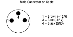
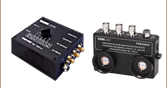
- 差分増幅フォトディテクタ(上記掲載)の交換用電源
- ±12 VDC出力
- 短絡回路を保護しオーバーロードを防ぐ電流リミット機能
- LED表示付きのOn/Offスイッチ
- AC入力電圧はスイッチ切り替え可能(100/120/230 VAC)
- 長さ2 mのケーブル、LUMBERG製オス型コネクタRSMV3付き
この±12 VDC安定化リニア電源LDS12Bは、上記掲載のPDBシリーズの差分フォトディテクタに付属する電源の交換用製品です。ケーブルに付いているコネクタは3ピンで、グランド用、+12 V用、-12 V用となっています(上図参照)。また、日本国内仕様の電源ケーブルが付属します。この電源は当社のPDAシリーズの増幅ディテクタ、PMMシリーズの光電子増倍管モジュール、APDシリーズのアバランシェフォトディテクタ、フェムト秒レーザ用オートコリレータFSACにも対応しています。